This article is more than 1 year old
Executing the DIMM sidestep: Movements in High Bandwidth Memory
Get the data out of memory faster
Analysis Getting data into and out of memory is like getting books into and out of bookshelves. The more books you can hold at once, the faster you can do the job. Someone able to hold only one book at a time is going to be far slower than another person capable of holding a stack of eight at a time or, with high-bandwidth memory (HBM) in mind, 1,024.
Samsung announced plans around second generation HBM last year – as did unlikely teammates Intel and AMD later in the year. And just a few weeks ago, Sammy announced it was mass-producing Aquabolt HBM2 memory. What is it and how did we get here?
Memory 101
Memory (RAM) is needed to hold the data that processors process. It is packaged into dual, inline memory modules or DIMMs which have a certain capacity, speed and bandwidth across a bus. Currently the most popular format seems to be DDR3 (Double Data Rate 3) and this is giving way to faster DDR4.
GDDR
With the rise of graphics and GPUs, the GPUs are separate from a host CPU and memory, think compute RAM, and need their own memory, video RAM. So standards came into being to evolve DDR3 RAM technology into graphics memory and GDDR4 and GDDR5 versions of that are based on DDR3 RAM. A GDDR6 version is being worked on, by suppliers such as Rambus, with a DDR4 starting point.
Rambus documentation says: “The GDDR6 interface supports 2 channels, each with 16 bits for a total data width of 32 bits. With speeds up to 16 Gbit/s per pin, the Rambus GDDR6 PHY will offer a maximum bandwidth of up to 64 GB/s.“
GDDR4 can operate at 2.8Gbit/s to 4Gbit/s per connecting pin at 1.5V.
According to Samsung, GDDR 4 chips operated at 16GB/sec overall bandwidth, while GDDR5 features a 32-bit bus, an 8Gbit die, and overall bandwidth of 32GB/sec (8Gbit/s/pin x 32 bit bus = 32GB/sec).
GDDR is not enough
Some applications need even faster access, up in the hundreds of Gbit/s area. Which are these?
Samsung mentions artificial intelligence, HPC (high-performance computing), advanced graphics, network systems and enterprise servers. That’s a wide spread – it is basically anything that thinks the extra cost for this speed is worthwhile. Let’s assume that the general enterprise servers and network systems side of this are not the main markets for now.
AMD and others saw a looming problem with GDDR meeting this need, and that was its power draw, with AMD stating: “GDDR5 can’t keep up with GPU performance growth GDDR5's rising power consumption may soon be great enough to actively stall the growth of graphics performance.”
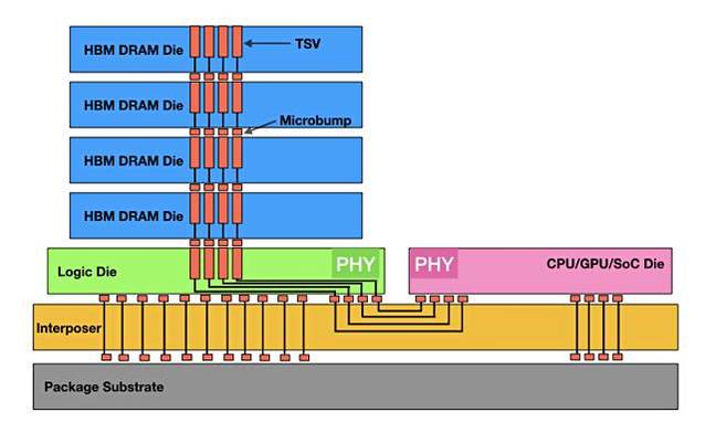
Also a large number of GDDR5 chips are required to reach high bandwidth. HBM was devised to overcome these limitations, with AMD saying; “HBM is a new type of memory chip with low power consumption and ultra-wide communication lanes. It uses vertically stacked memory chips interconnected by microscopic wires called "through-silicon vias," or TSVs.”
Hybrid Memory Cube
Micron and others developed a competing stacked DRAM concept, the Hybrid Memory Cube (HMC), with Micron saying: “Hybrid Memory Cube (HMC) is a single package containing four DRAM dies and one logic die, all stacked together using through-silicon via (TSV) technology.”
HBM is seemingly being used in preference to that, for example by Nvidia – so what of the HMC idea? The most recent news on the HMC website is dated November 2014 (PDF). Micron’s 2GB short-reach Hybrid Memory Cube product has a datasheet dated January 2013*.
HBM gets its extra speed by stacking DRAM layers in a pile, four initially and now eight, and getting them closer to the processor through using an interposer rather than a general data bus. That means the memory on-chip surface area is smaller than with eight separate dies, and power can be saved.

The HBM stacking and Interposer scheme
There have been three HBM technology iterations.
| HBM 1 | Gen 1 HBM 2 | Gen 2 HBM2 | |
|---|---|---|---|
| Die stack layers | 4 | 8 | 8 |
| Package capacity | 4GB | 4GB | 8GB |
| Package bandwidth | 128GB/sec | 256GB/sec | 307GB/sec |
| x4 | 512GB/sec | 1TB/sec | 1.23TB/sec |
Samsung's gen 1 HBM2 product was called Flarebolt and provided either 1.6Gbit/s @ 1.2V per connector pin or 2Gbit/s @1.35V per pin. Aquabolt bumps that up to 2.4Gbit/s per pin @1.2V, so enabling the 307GB/sec package bandwidth.

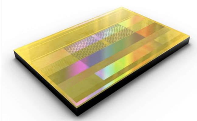
Samsung Aquabolt HBM package.
The SK Hynix HBM2 product provides 2Gbit/s per pin @1.2V, giving Samsung a performance edge.
Our sister publication, The Next Platform, has noted Intel is getting ready to finally bring its “Lake Crest” deep learning chip – which will include 32 GB of 3D-stacked HBM2 – to the market.
Applications like deep learning require so much processing of so much data that it has to be done with fast memory for deep learning run times to be acceptable.
Will this technology spread into the general server market?
The costs of mass bit extraction to and from memory has to be affordable for general server use of 3D DRAM.
If a supplier manages to develop a stacked DRAM DIMM then memory capacity generally could shoot up. However the expense of this could be so great that customers prefer to bulk out DRAM with 3D XPoint or some other storage class memory tech that is more affordable than pure DRAM and still boosts host server performance substantially. ®
* We have asked Micron for a Hybrid Memory Cube briefing.
