This article is more than 1 year old
Prepare for ReRAM speed! Crossbar samples SMIC chips
16nm? Lower. 10nm? Lower. You cannot be serious
ReRAM startup Crossbar has sample ReRAM chips from SMIC that are currently undergoing evaluation.
SMIC is using a 40nm process and there are plans for a 28nm process in development but Crossbar envisages scaling at least to 16nm and 10nm but then lower.
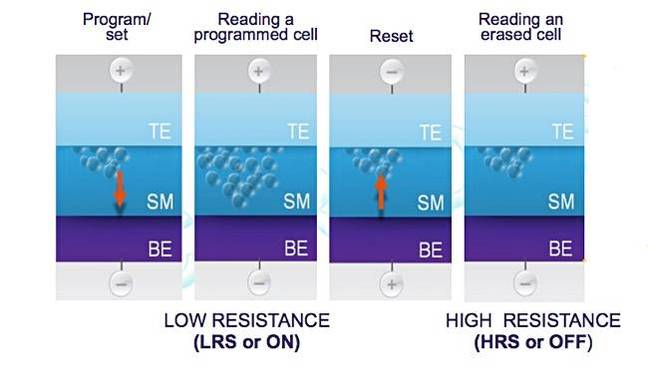
The chip design uses non-conductive amorphous silicon (a-SI) technology. There is a switching layer between top and bottom electrodes and the resistance of this layer to passing electric currents is based on ionic (silver) metal motion. The resistance is changed when a sufficient voltage is applied between the two electrodes which cause nano-filaments of ions to form between the electrodes.
The company says individual cells can be controlled by a transistor in a 1 transistor per ReRAM cell – 1T1R – arrangement. Transistors have size constraints. Alternatively, and more cost-effectively, many ReRAM cells – up to 2,000 say – can be controlled by a single transistor if each cell has an in-cell selector mechanism that can select or not select individual cells – a 1TnR scheme.
This is done by implementing a crossbar scheme similar to Intel's 3D XPoint memory. Up to 16 levels have been suggested as being feasible.
The 1T1R scheme offers the lowest latency, while the 1TnR scheme has the best area density efficiency. We might imagine a 1T1R scheme would be used in embedded memory applications, involving caching, with the 1TnR design used in storage drives such as SSDs in formats such as M.2 or even NVDIMMs.
Crossbar tells us that scaling ReRAM cells down to sub-10nm level will not adversely affect filament formation and destruction, unlike with NAND flash where cell scale-down results in too few electrons to retain an applied charge, causing cell bit value degradation. As well as this, Crossbar claims its ReRAM chips have 100 times lower read latency and 20 times faster write performance than NAND Flash, with Crossbar saying: "ReRAM-based SSD will provide lower and more deterministic read latencies, in the range of tens of microseconds."
A random 4K read from an SSD can take 150μs but caching and access stack simplification can shrink that with, for example, an NVMe PCIe SSD read taking 110μs and a write 30-50μs. A Micron Optane (3D XPoint) has a 10μs read latency and 20μs write latency, we understand.
All of which means ReRAM has a bit of a hurdle to get over.
ReRAM is also byte-addressable instead of being block-addressable. Its design can involve small pages which "simplifies drastically the complexity of the storage controller by removing a large portion of the background memory accesses required for garbage collection".
Crossbar's ReRAM technology does not require any erase operation prior to being programmed, and should have vastly greater endurance than 2D MLC and TLC NAND at 15nm cell sizes. We don't understand how its endurance compares to 3D NAND, which uses larger cell lithography sizes.
Back in December 2014, Crossbar said it had solved a sneak path current problem, which affected cell content readability. In September 2015, it was given $35m D-round cash to fund commercialisation of the technology, following a $25m round the year before. First production was then targeted by the end of 2016.
Crossbar licenses its technologies to foundries and is talking to potential but unrevealed partners about discrete ReRAM memory-style chips.
The competition between Xpoint, ReRAM and NRAM is hotting up as vendors and technology startups jostle to strike their claims in the DRAM-flash performance gap.
A 2014 ReRAM PDF slide deck might be an interesting read, as might this one. Expect more slight dribbles of Crossbar news later this year. ®
