This article is more than 1 year old
Flash breaks free from the storage flat earth society
An exit route from the trap
Samsung and V-NAND

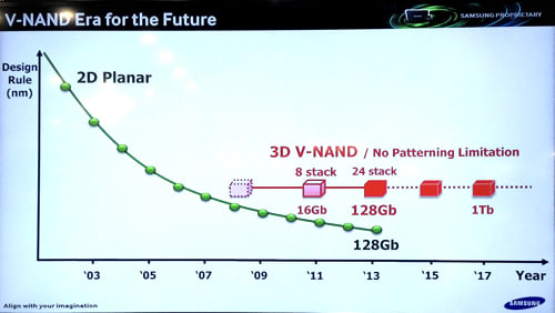
Samsung's 3D V-NAND layers
According to one Samsung V-NAND timescale chart it has 3D NAND overlapping the planar stuff from 2011/12 and 2D NAND stopping with a 128Gbit chip in 2014. At that point it has a 128Gb 24-layer product.
Samsung announced mass production of its 24-layer 3D V-NAND dies in August last year, and has just announced a 1TB 850 EVO SSD 32-layer V-NAND chip using TLC or 3bits per cell flash with a 40nm-class geometry.
Its endurance is 150TB written over the life of the drive and it has a five-year warranty – pretty good for a client-class SSD.
V-NAND timescale
Samsung has a 3.2TB NVMe PCIe SSD using its 3D V-NAND technology. "Samsung plans to aggressively introduce V-NAND-based SSDs with even higher performance, density and reliability in the future," says Samsung Electronics memory marketing vice president Jeeho Baek.
El Reg can envisage doubling and tripling and potentially quadrupling this with 3D NAND as the technology develops. Certainly SanDisk’s Fusion-io acquisition has aggressively driven up PCI flash card capacity in the past with 10TB ioDrive products, so it might be thinking of 20 to 30TB flash cards using its 3D NAND tech.
SanDisk and Toshiba
Toshiba, which partners SanDisk in its flash foundry operations, developed a 16-layer, 32Gb 3D MLC prototype flash chip in June 2009, two years after starting work.
Its technology, which it calls P-BICS (pipe-shaped bit-cost scalable), featured a U-shaped layout of cells. It used 60nm cell geometry, a far cry from today’s leading-edge sub-20nm geometries, and the chip size was 10.11mm x 15.52mm.
There has to be a means of accessing the stacked layers, and this is done by creating through-holes or vertical pipes between them. Due to pipe wall insulation problems the chip was actually made from two eight-layer components stacked one on top of the other.
Around the end of 2012 Toshiba said it had 16-layer chips with a 50nm vertical channel. Toshiba calculated that its P-BICS chips were cheaper to make than 2D flash chips (at the same capacity) when the layer count surpassed 15.
Toshiba at the time suggested we would see 128Gb and 256Gb prototype samples in 2013, engineering samples in 2014 and volume shipments next year. In 2013 SanDisk CEO and co-founder Sanjay Mehrotra said he thought meaningful production of 3D technology, referring to BiCS kind of 3D NAND technologies, is two to three years out.
There was scope, he thought, for further reduction from what was then the leading-edge 19nm cell geometry used in 2D NAND. After that the scaling trap would hit and it would be more profitable to transition to 3D NAND.
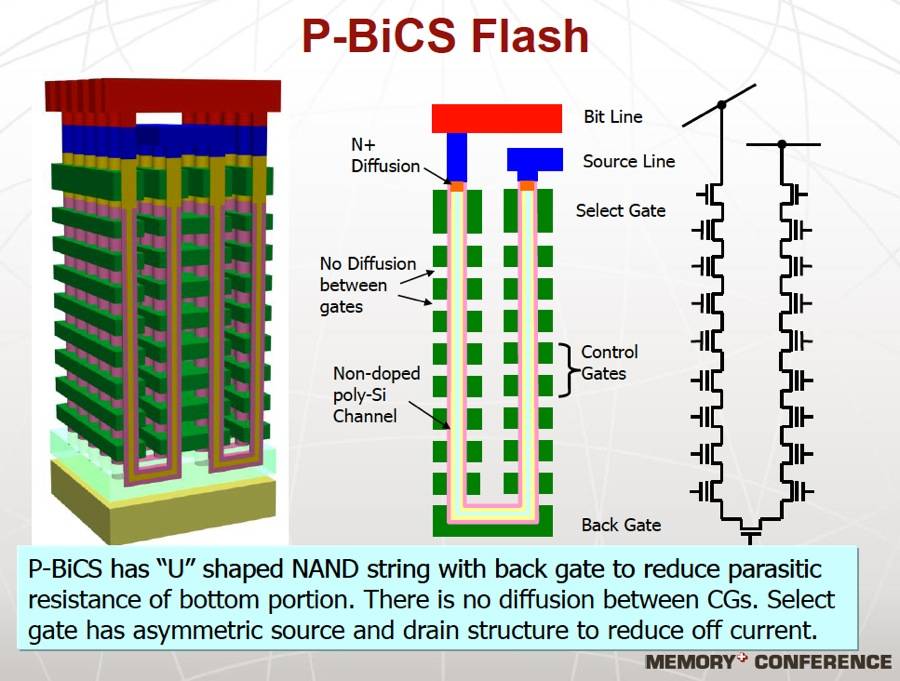
Toshiba P-BICS 3D NAND concept
Intel and Micron
A month or so ago Intel, which partners Micron in Intel Micron Flash Technologies, strutted its 3D NAND stuff. It talked about:
- 32 planar layers
- c4 billion interconnect pillars between the layers
- Up to 32GB of capacity in a die using MLC (2bits/cell) NAND
- up to 48GB using TLC (3bits/cell) NAND.
We can view this as a joint Intel/Micron statement. An Intel spokesperson said there could be could be 1TB capacity 2mm thick mobile device flash products using the technology, suggesting that tablet and mobile phone storage capacity could increase.
A compendium view of the manufacturers’ 3D NAND timescales is given in this Stifel Nicolaus chart:
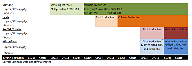
Stifel Nicolaus 3D NAND timescales
Come 2017 we should see a vast increase in in-memory computing by servers, the continued erosion of disk drive array usage for primary data and a growing incidence of active archival stores using 3D TLC flash to provide very large capacity flash WORM-type storage: write once and read seldom, but read darn quickly when you need to access archived data, with no waiting to bring a tape online or start up a spun-down disk.
At this tail end of 2014 we are looking at a three-year lag before 3D NAND becomes mainstream technology and substantially alters the IT application landscape.
The flash flat earth society will end and we will revel in huge flash data stores. Bring it on. ®
