This article is more than 1 year old
Teeny, tiny state machine could BREATHE NEW LIFE into Moore's Law
'Densest system ever'
A team from Harvard University and the non-profit military contractor The MITRE Corporation are claiming a miniaturisation breakthrough with what they say is the smallest finite state machine ever built.
Their “nanoFSM” is, the group claims, “the densest nanoelectronic system ever built”. It comprises hundreds of transistors built of non-volatile nanowires that retain their state without power.
This, the researchers say, is the first time such a technology has produced a system that can be described as a complex and programmable nanocomputer.
Working with features sometimes smaller than a nanometre, the researchers first assembled the nanowire transistors into tiles, then organised the tiles into circuits, and finally provided the circuits with connections to the outside world. As the image below shows, connectivity needs far more space than the nanoFSM itself.
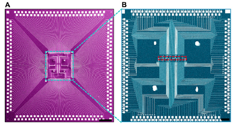
Left, the complete chip (scalebar 500um); right, the inner region (scalebar 100um).
The red square outlines the three nanoelectronic tiles.
Image, Jun Yao et al, Harvard U and MITRE
MITRE's Shamik Das, who heads the organisation's Nanosystems Group, said: “It was a challenge to develop a system architecture and nanocircuit designs that would pack the control functions we wanted into such a very tiny system”.
From the MITRE system architecture, the Lieber Research Group at Harvard undertook the nano-scale build (Charles Lieber, who heads the Harvard team, is corresponding author of the PNAS paper that describes the research project).
As the research abstract notes, the nanoFSM includes both computing and memory elements, “which are organised from individually addressable and functionally identical nanodevices, to perform clocked, multistage logic.”
While not presenting this as the whole solution to the Moore's Law problem, MITRE's chief scientist for nanotech James Ellenbogen said “I believe that they do incorporate important steps forward in two of the key areas the electronics industry has been focused upon in order to extend Moore’s Law”.
The technique involved coating a substrate with a resist coating that was “combed” to provide a substrate to grow the nanowires. The resist was then removed and a mask pattern applied so the nanowires could be trimmed. After the mask is removed, the prepared surface is ready for circuits to be fabricated.
The latest project builds on work in 2011 by the same team, which demonstrated the building of a single nano-scale logic tile. ®
