This article is more than 1 year old
Memory vendors pile on '3D' stacking standard
HMC 1.0 in the wild
More memory responding faster in a smaller footprint: that's what chip vendors are hoping to achieve with the announcement of the HMC 1.0 specification.
The standard, available here, sets down the specs for memory chip stacking using through-silicon vias (TSVs). In other words: individual memory dies, stacked vertically on top of a controller, with connectivity through the silicon.
It is, in other words, a combination of manufacturing process and logical organisation. The logic is necessary: merely stacking memory locations would merely create a large physical memory with an I/O bottleneck.
As the HMC concept diagram below illustrates, portions of each layer would be organised as positions, grouped into vaults, with the base layer handling the organisational logic (irrespective of how individual manufacturers handle physical organisation).
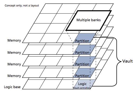
HMC 1.0 logical organisation. Source: Hybrid Memory Consortium
That logical organisation – as well as boring details like device pinout – that's important to the initiative, since it means devices should be interoperable regardless of the on-chip design or manufacturing approach the vendor takes.
The specification claims up to 15 Gbps SerDes I/O, supporting multiple 16-lane full-duplex links and, according to the HMC Consortium, provides “more than 15 times” the performance of today's DDR3 modules at “70 percent less energy” than DDR3 DRAM technology.
That performance, the consortium says, is important to stop memory becoming a worse performance bottleneck than it already is, in an age where (for example) GPU-based supercomputers are handling truly stupendous data sets.
HMC 1.0 is supported by founders Samsung and Micron, along with HP, ARM and Hynix.
The publication of HMC 1.0 will also pressure microelectronics standard-setter Jedec to accelerate its TSV and 3D memory efforts. It has an addendum to the DDR4 standard in the works (currently describing the initiative as “making good progress”), and has published its Wide I/O JESD229 standard.
Foundries, however, aren't waiting to see which standard wins: they're working hard to position their 3D capabilities whichever way the die falls. Globalfoundries announced its first functional 20nm TSV chips out of its New York facility, while IBM, Samsung, Tezzaron, TSMC and UMC are all working on TSV capabilities.
According to Chip Design magazine, volume shipment of 3D devices won't happen until 2014 or 2015. At this point, foundries are still competing to solve the fabrication challenge – for example, settling on which manufacturing process is going to deliver reliability, yield and low production cost.
Globalfoundry's approach is to insert the TSVs between the “front end of line” and “back end of line” processes (FEOL and BEOL respectively), so that the vias themselves aren't exposed to high processing temperatures; this allows boring old copper to be used as the via. Tezzaron, on the other hand, uses tungsten for the vias – more expensive than copper, but it claims that the material minimises thermal mismatch. ®
