This article is more than 1 year old
Hynix figures to win on NAND by being smaller than rivals
Ha ha, with my 15nm tech I run between your legs, giants
Hynix, which trails Samsung and Toshiba in the flash market, is trying to gain ground on them with a 20 per cent better NAND process.
As measured by iSupply, Hynix had just 13.5 per cent by revenue of the NAND market in the second 2011 quarter, with Samsung leading with its 41.6 per cent, Toshiba second with 28.7 per cent, and Micron third with16 per cent.
A key aspect of flash chip costs is the number of dies that can be produced from a wafer and the smaller the die the higher the yield from wafers. This means that hand-held smart, Internet-connected devices, like phones and tablets, and ultrabooks as well, could have more storage capacity inside their space-constrained cases.
Currently the NAND fab operators are moving to sub-30nm manufacturing processes, with 20nm processes being the advancing edge. Micron has developed a 20nm process as has Samsung, while Toshiba has gone 1nm further with a 19nm process.
Hynix has jumped them all, with a 15nm process, 21 per cent smaller than Toshiba's 19nm one, which it described at the International Electron Devices Meeting in Washington, DC, last week. Tech-On and other media presented details from Hynix' pitch at IEDM.
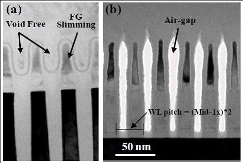
Hynix 15nm NAND process and the air gap.
The company said there were problems in both the bit line and word line directions with this 15nm process. The word line is used to control access to the cell with the bit line being used to transfer data in read and write operations. There was interference between bit lines in the world line direction, and Hynix reduced this by a fifth through increasing the area in which control gates are set and shrank the width of the floating gate in a direction parallel to the word lines.
In the bit line direction there was also increased risk of electrical charge leakage from a floating gate when writing data. This was sorted by increasing an insulating air gap (image above) between adjacent world lines. Hynix also increased the voltage by about 2V to the world line adjacent to the word line being used in the writing operation. This reduced the leakage risk and increased the writing speed; a neat result.
Hynix said its 15nm technology was suitable for 2-bit multi-level cell NAND. If the company can productise its prototype 15nm technology then it could be delivering NAND die with a significantly lower cost-to-manufacture than its competitors and be able to lower its prices and/or increase its profits.
Hynix will be telling suppliers of smartphones, tablets and ultra books that they could have higher flash storage capacity in the same physical space by using its 15nm NAND. ®
