This article is more than 1 year old
BREAKTHROUGH: Feisty startup slashes chip power by 50%
SuVolta to Intel: 'The future is the $10 chip, not the $200 chip'
Three layers, no waiting
Another major transistor bugaboo is voltage variability – and from SuVolta's point of view, taming variability is the key to lower voltages. It doesn't take a PhD chip boffin to understand that the lower the variability in a transistor's operating voltage, the lower the overall voltage supplied to a million-transistor chip needs to be to ensure that all the transistors will fire up when asked to.
Since reducing a chip's operating voltage is key to reducing its overall power consumption – along with other niceties such as intelligent power managment and the like – Shifren and the SuVolta team focused on developing a transistor that could operate at low, steady voltages and still be manufacturable in existing fabs with very little equipment modification.
One sticking point, however, was that SuVolta wanted to build a transistor that could be operated at multiple voltages. Foundries, after all, have customers with different needs – unlike Intel, which builds its own chips in its own fabs, and thus has less of a need for the ability to create chips that operate at a broad range of voltages.
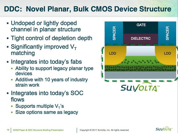
What SuVolta came up with was a new way of building a transistor's channel – its pathway for current – that cut its voltage variablity nearly in half, thus allowing the overall voltage to be lowered, and that permitted the manufacturing process to create a broad range of transistors at a broad range of voltages.
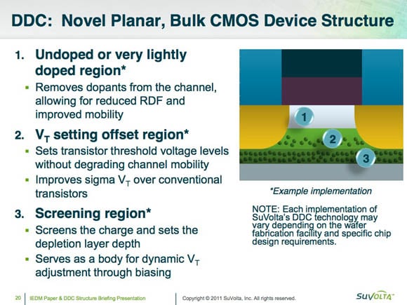
A DDC transistor's channel is a three-layer parfait. The layer in direct contact with the transistor's gate, or on-off switch, is undoped or very lightly doped silicon. The lack of dopants (impurities added to increase conductivity) in this layer avoids the dreaded volage-variability-inducing random dopant fluctuation (RDF), as well as allowing the channel to be highly depleted.
A second layer beneath the no-or-low dopant layer sets the transistor's "it's time to turn on now" threshold voltage (VT), which allows the DDC transistor to meet its objective of being fabricated with a broad range of voltage requirements. This is accomplished by adding a medium dose of dopants that control the voltage properties of the first channel.
"By changing the dose in that layer," Shifren says, "we're able to apply a potential to the channel non-locally, from underneath the channel. So instead of applying the potential in between the source and the drain, or within the channel, we actually apply it from underneath using layer number two."
Although Shifren admits that VT variations increase when the second channel cranks up the first channel to a higher VT, "it's significantly less than if we put all that dose into the [first] channel."
The third layer – which SuVolta calls the "screening region" – is more highly doped layer that terminates the depletion depth. "You don't want your depletion depth going way too deep into the device," Shifren says. A secure termination of the depletion depth assures that the DDC exhibits fully depleted behavior.
"The reason why people do FinFET or FD-SOI is to have that depleted behavior, and this allows us to have that depleted behavior," Shifren told us.
The other advantage of the third layer's termination of the depletion region brings us back to the goal of reducing VT variability. "That depletion region is going to be very uniform across the entire part, and it's this uniformity that helps us to achieve the excellent sigma VT" Shifren said, referring to DDC's low standard deviation of all of a chip's transistors' threshold voltages (σVT).
If, by the way, all this doping, depletion, and deviation is not quite geeky enough for you, you can find a more complete explanation in SuVolta's technology brief, "Transistor VT Variation, VDD Scaling, and Leakage Power". Knock yourself out.
By now, you may very well be asking, "What's in it for me?" Fair question.
Should SuVolta's DDC transistor prove as impressive in reality as it is on paper, its 50 per cent decrease in voltage variation should enable a concomitant 30 per cent reduction in power supply voltage. Simply put, a lower power supply voltage means less power needed, less power needed means longer battery life in your mobile devices.
Also, Shifren assured us that creating DDC-transistor chips won't require expensive foundry retooling and process-flow changes, but instead minor tweaks to existing bulk planar CMOS chip-baking tools and techniques. Cheap manufacturing means cheap chips, and cheap chips means cheap consumer-electronics gadgets and gizmos
Finally, although stuffing servers with cheap chips based on DDC transistors could also help massive data centers reduce their power bills, at this point in time SuVolta is aiming at the mobile SoC market.
"The market's now moving to a point where you're really going to be driven by the $10 chip and not the $200 chip," Shifren told us, "so these fancy 3D technologies and FD-SOI products, they're going to be too expensive for where the market is going."
If SuVolta's work with Fujitsu pans out, Intel's "fancy 3D technology", tri-gate, might have a strong competitor facing it at the low end of the market – a place where Chipzilla has yet to find success. ®


