This article is more than 1 year old
Elpida aims to issue $1bn of paper to fund re-tooling
DRAM it, we've been left behind
Elpida needs to raise nearly one billion dollars to fund a transition into making memory for smartphones and tablet PCs, relying less on PC DRAM in the future. Revenues from DRAM have fallen short of what's needed and Elpida will issue new shares and convertible bonds to pay for the direction change.
It's a massive amount of money – $998m or 79.67bn yen – and investors are worried about share dilution. Perhaps they should be more concerned about the ultimate survival of Elpida as Japan's only DRAM manufacturer.
An Elpida statement said that the DRAM industry faces drastic changes. It needs to shrink its production processes, focus on through-silicon via (TSV) memory, and research new memory technologies, as well as moving into the smartphone and tablet PC memory markets.
The company's Hiroshima plant will be equipped with 30nm and 25nm DRAM wafer production processes. These will enable more memory chips to be produced from a wafer and so lower memory costs.
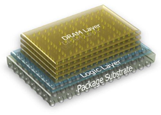
Through-silicon via
The plant will also get new TSV process manufacturing lines, in which stacked memory chips have vertical connections (vias) cut into them to enable communications between the memory cell layers.
TSV technology is also being pursued by Micron. Dean Klein, Micron's memory systems development VP, attended ISC at Hamburg, and described its Hybrid or Cube Memory: "3D DRAM connected with thousands of through-silicon vias."
He said he thought this could provide both high-performance logic and hundreds of GB/sec bandwidth.
"Every CPU in a high-performance computing configuration could have some amount of hybrid memory, with very low latency and very high bandwidth," said Klein.
A bandwidth of 20x DDR3 bandwidth was also mentioned.
Klein said he foresaw a memory hierarchy for HPC which started off with Hybrid Memory, then went to DDR4 DRAM, then to a Phase-CHage Memory (PCM) tier, then NAND, and, finally, off to spinning disk.
Klein said that every DRAM part of a DIMM was fired up to get at 32-bits of data from one section of DRAM. With the Hybrid Memory Cube you only needed to active the section of DRAM holding the desired bits and in that way, you save electricity: "And it's faster too."
DRAM replacement technology
Thirdly, Elpida will also fund research and development into new memory technologies and next generation processes.
These technologies would replace or augment DRAM and could be post-NAND processes such as FE-RAM, Memristor, or PCM, which all generally combine DRAM or near-DRAM speed, bit addressing, and NAND's non-volatility. None are close to production yet, although promising advances are being made with PCM and Memristor technology.
Fourthly, Elpida will pay off some long-term debt.
The basic problem is that Elpida is losing out in the traditional DRAM market and hasn't made sufficient profits to fund the moves it now needs to make to stay competitive with the likes of Hynix, Micron and Samsung. They are positioned to move more rapidly than Elpida into the multi-tiered, multi-technology, post-DRAM world.
Elpida's plan appears to be to make wafers on smaller processors and so decrease DRAM costs; to implement TSV technology to increase memory chip capacity, energy efficiency and speed; and then have a next-generation memory technology ready when ordinary DRAM runs out of steam.
Any one of these three bets could fail to deliver the goods, with Elpida having to then seek salvation through a merger or an acquisition. ®
