Original URL: https://www.theregister.com/2014/01/14/amd_unveils_kaveri_hsa_enabled_apu/
AMD's 'Revolution' will be televised ... if its CPU-GPU frankenchip Kaveri is a hit
Graphics and x86 cores are all just 'compute units' now for our games, videos and apps
Posted in Personal Tech, 14th January 2014 13:00 GMT
AMD has released its long-awaited Kaveri processor, the first accelerated processing unit (APU) to incorporate both on-die CPU and GPU cores in a heterogeneous system architecture (HSA) with a shared memory architecture.
"We're going to need to create a new term," AMD product CTO Joe Macri said at a Kaveri briefing, "because HSA has really changed what can be done on the graphics part of the die."
That new term, Macri explained, is compute cores. "The compute cores can either be CPU cores or graphics cores," he said. "We based them on the historical definition of what a CPU is," meaning that in an HSA system, each compute core – CPU or GPU – is programmable, capable of running at least one process in its own context in its own virtual memory space, and do so independently from all the other cores on the 2.41-billion transistor, 245mm2 die.
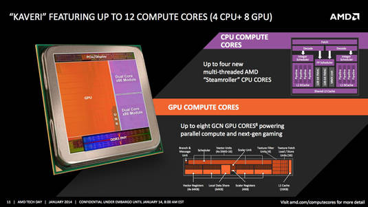
The four CPU cores and the eight GPU cores in the HSA-enabled Kaveri processor can each run its own thread, drawing data from a shared memory space. Kaveri, Macri explained, should therefore be regarded as a 12-core processor.
"We want to be able to talk about core count," he said, "because when we describe the device, core count represents throughput to first order [tasks]. There are other metrics of throughput that can also be applied, but we thought it was very important to be able to talk about a device, talk about the number of cores, and have the end user in the technical community to start picturing in their mind what the capabilities of this device really are."
So from now on in the new HSA environment, AMD would like you Reg readers – members of the technical community that you are – to subsume the terms CPU and GPU into the larger, more inclusive term of compute cores. "It's going to become part of our dictionary, our technical dictionary going forward," Macri said.
Not that the 12 compute cores in Kaveri are identical – far from it. Four of them are CPU cores based on AMD's "Steamroller" architecture, while the other eight are GPU cores based on the company's "Graphics Core Next" (GCN) architecture.
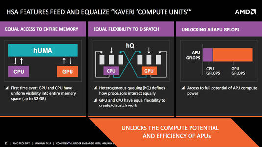
What ties them together and makes them cooperative compute cores is HSA, comprised of hUMA (heterogeneous uniform memory access) and hQ (heterogeneous queuing). "An unprecedented amount of parallelism is available in Kaveri," Macri claimed, "when you literally have 12 unique threads running on this design. First time ever."
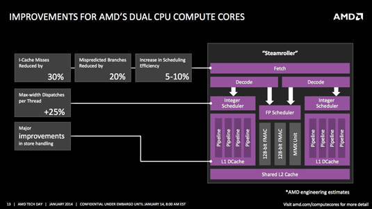
The CPUs are first among equals, he said, because they're the most general-purpose cores, and the version of the Steamroller cores in Kaveri have been tweaked to improve efficiency and performance.
On the die, memory matters
For one thing, Macri told The Reg in a sit-down after the group briefing, AMD has doubled the size of the branch target buffer in Kaveri over that of its predecessor, Richland.
"It also has one new cute feature in that when it misses in the [instruction] cache now, we kick off a prefetch," he said. "And prefetches are neat in that if they're 100 per cent accurate, then it's super-cool. Getting a memory reference out early helps the memory controller slide it into a place that's idle."
Improving the prefetching of instructions from RAM helps further alleviate the pain of an instruction cache miss: this happens when a core attempts to touch program code outside the cache, forcing it to stall while waiting for the memory controller to copy fresh instructions into the cache. However, by being a bit smarter, "when you shoot a prefetch out, it's like, 'hey, you can take a little longer'," he said.
Such tweaks have allowed Kaveri's designers to boost the CPU's overall instructions-per-clock (IPC) performance by helping out the memory subsystem – which, by the way, has a clock rate of 2400MHz, up from Richland's 2133MHz.
And speaking of memory, Kaveri has two 64-bit, fully independent memory channels. "We do stripe across them," Macri told us, "especially for the memory that's allocated for high-bandwidth needs like graphics."
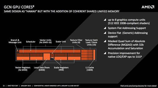
AMD's Graphics Core Next finally makes it onto a processor die along with CPU cores (click to enlarge)
Compared to discrete GPUs, a 128-bit-wide memory bus might seem – well, does seem – a bit paltry when compared with AMD's most powerful discrete GPU, which has a 512-bit bus. But as Macri points out in defense of the narrower path, Kaveri has just eight GPU cores to feed, whereas the hefty discrete-memory GPUs have more.
"We are a little light on memory bandwidth for graphics," he said, "but we're perfect, I think, on the compute side – or very close to being very well balanced on the compute side."
There are other reasons for the narrower memory bus, not the least being cost – both in terms of package cost and die real estate. A 64-bit memory channel uses about 118 pins for data, address, control, and clocks, he told us, and 0.8mm2 per byte is a good rule of thumb for additional die size. So if you wanted to add another 64-bit memory channel, you'd need to add about 6.5 to 7 mm2 of die real estate and more than 100 extra pins to the package, driving up both cost and size.
"Things just start adding up so that you can't afford it," he said. "And then in small-form factors, there's only enough room in here to have a 128-bit memory bus. And we really optimized Kaveri around ensuring that it can go into a small-form factor all the way up to the desktop. If we were only designing for desktop, I would have probably added another memory channel."
Macri told us that Kaveri's designers did "as much as possible to utilize that memory bandwidth as well as possible." For example, at the back end of the graphics pipes there's a local data share [PDF] between the different stages to reduce the need for having to go off-chip in search of data. In addition, he said, "GCN has a nice array of on-die buffers: L1 caches, L2 caches, local data stores. These all help."
When is 28 nanometers faster than 22?
Kaveri is baked in a 28-nanometer, planar, bulk silicon process, which is nowhere near as efficient as state-of-the-art FinFET (what Intel calls "Tri-Gate") or even the less-than-TriGate, more-than-bulk – and somewhat expensive – silicon-on-insulator (SOI) process that was used in Kaveri's predecessor.
There were reasons to go with 28nm rather than 22nm, Macri told us, that were discovered during the design process. That process was run by what he identified as a "cross-functional team" composed of "CPU guys, graphics guys, mixed-signal folks, our process team, the backend, layout team."
That cross-functional crew identified a boatload of process variants, and members of the team each ran tests based on their areas of interest, examining such factors as power curves and die-area needs.
"What we found was with the CPU with planar transistors, when we went from 28 to 22, we actually started to slow down," he said, "because the pitch of the transistor had to become much finer, and basically we couldn't get as much oomph through the transistor."
The problem, he said, was that "our IDsat was unpleasant" at 22nm, referring to gate drain saturation current*. In addition, the chip's metal system needed to be scaled down to fit within the 22nm process, which increased resistance.
"So what we saw was the frequency just fall off the cliff," he said. "This is why it's so important to get to FinFET."
Moving to 28nm was best for the CPU in a bulk planar process, he said, and moving from the previous 32nm process to 28nm gave the GPU cores a "nice little boost." That said, "It wasn't as nice as I would have liked to have gone for the GPU, which is as small as you could make it."
The process in which Kaveri is baked, in fact, is a compromise between the needs of the CPU and GPU cores – it's a balanced system. But it's also a dual-mode system: the chip can use its GCN cores for graphics, or it can be coupled with a discrete graphics card. In the latter mode, Kaveri's GCN cores can pick up CPU chores, thanks to the HSA architecture.
HSA, Macri said, allowed Kaveri's designers to make optimizations that were "better for the notebook, and didn't hurt the desktop because we still kept the silicon alive when we're on desktop" and using a discrete graphics card.
"Let's say you're playing a game and using the discrete to drive all the visuals," he said. "You can now use the compute in the APU to drive all the physics. And you don't run into the problem like we've run into in the past of, 'Oh, damn – I do a bunch of physics on my GPU and my frame rates start to go down. I get great effects, but if I'm in a first-person shooter, I want high frame rates.' You want high frame rates with great physics – that just gives you better game play."
But wait! There's more
In addition to the combination of CPU and GPU cores in the new HSA-enabled shared category of compute cores, Kaveri adds some specialized fixed-function accelerators, as well.
"The reason we put accelerators on the device is that we want to keep the CPU and GPU free to do things that only are available via general-purpose computing," Macri said during the briefing. For example, he said that the industry-standard H.264 video codec shouldn't clog up the CPU and GPU cores, and is an ideal candidate for a specialized accelerator that can perform such tasks using less power.
To handle H.264 encoding, Kaveri has an on-die video encoding engine (VCE). So did its APU predecessors, but Kaveri's version has been amped up with new capabilities, including what Macri called significantly improved text rendering and 60GHz wireless docking (that's not a typo).
There's also unified video decoder (UVD) hardware that handles a variety of video codecs: H.264/AVCHD, VC-1/WMV profile D, MPEG-2, MVC, MPEG-4/DIVX. Its predecessor UVD 3 could handle those, as well, but AMD promises that Kaveri's UVD 4 offers "improved error resiliency" for H.264/AVCHD to guard against video freeze-ups.
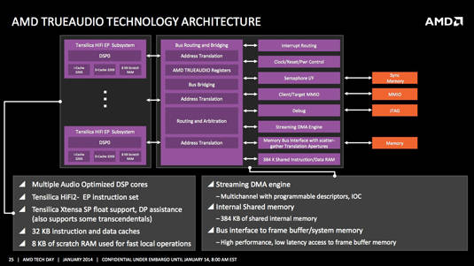
There's also a new audio coprocessor that AMD dubs TrueAudio, which has multiple digital signal processors, its own on-die storage and DMA agent, and its own programming interface so that developers can tightly control sound quality and direction.
Macri emphasized that TrueAudio takes up only a small bit of the Kaveri die. "The big die area is for the CPU and the GPU," he said. "That's left free to do things that only they can do." The TrueAudio accelerator takes only a comparatively tiny slice of real estate, but it frees up the "maximum amount of compute area for all the good stuff."
Work on all of Kaveri's goodies – HSA, hUMA, hQ, CPU, GPU, accelerators – Macri said, started about four years ago, and has resulted in new cores, new compute architecture, new power management, new CPU/GPU balanced process, and new accelerators. "We had to predict the future," he said, speaking to the assembled press at the briefing, "and you guys are going to tell us, did we predict right."
Well, no, we're not. As much as we press folks like to think that we have the power to influence the market to a great degree, we have to disagree with Macri on this point.
It's you, Reg reader, and your compatriots in the marketplace who are going to decide whether AMD and its new Kaveri processor correctly judged the needs of the next generation of computing, not the tech press.
We look forward to learning your verdict, which will decide whether Kaveri warrants the catchphrase of AMD's briefing: "Welcome to the Revolution." ®
* You can find a crash course in silicon gate saturation current and related electronic engineering here [PDF].
