Original URL: https://www.theregister.com/2012/07/16/ibm_power7_plus_preview/
IBM's new Power7+ hotness - we peek through the veil
Saucy internet pictures reveal Big Blue secrets
Posted in Systems, 16th July 2012 08:00 GMT
Analysis A few weeks ago, El Reg told you that IBM was getting ready to start talking about its future Power7+ and System zNext processors at the Hot Chips conference at the end of August. Like you, I am an impatient sort when it comes to getting some insight into future processors from any vendor, and I like to poke around and see what I can find out about these chips as soon as possible because it is interesting and useful to know as much as possible as soon as possible.
I like rummaging around the Internet for processor roadmaps and such as well, and occasionally I find stuff that at least assures us there is a future for any particular technology - in this case the Power processors and the IBM i, AIX, and Linux systems that depend upon them as their compute engines.
Here's a tidbit I found about investment in Power iron. In a presentation from February 2011 (PDF) by Peter Nimz, product manager for Power Systems at IBM Deutschland, Big Blue said that it had invested $3.2bn in Power7 systems over the past 3.5 years. That's an average of $915m a year for a product line that ranges from $3.5bn to $4.5bn a year in total sales, and that is a pretty substantial investment. It no doubt includes chip design, the Power Systems division's allocation for overhead for chip fabrication development, and the actual server engineering, too.
IBM could do a better job putting out a long-term public roadmap for its Power and mainframe processors, but as the dominant player in the Unix racket now, Big Blue doesn't feel it needs to do that: while Oracle, which bought former Unix leader Sun Microsystems, has to put out a roadmap to demonstrate its commitment to the Sparc architecture. Hewlett-Packard has left its Unix and proprietary systems future largely in the hands of Intel - which it has apparently been paying for years to continue Itanium development as well as manufacturing - and Oracle, which has put a serious damper on Itanium by not supporting its current or future software on future Itanium processors.
We know that Power7+ is coming sometime toward the end of this year, and that it will be implemented using 32 nanometer processes at IBM's East Fishkill, New York, chip fab.
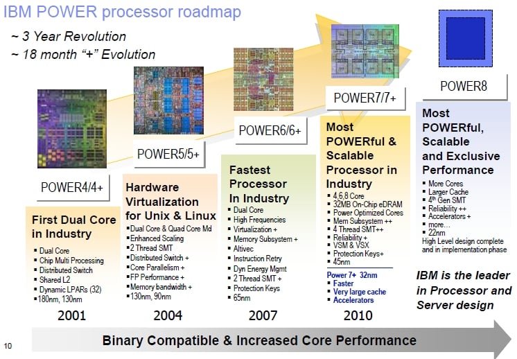
IBM's Power roadmap circa the summer of 2011 (click to enlarge)
As you can see from the roadmap, the move from Power7 to Power7+ involves a process shrink from 45 nanometers, which means IBM can cram a lot more transistors onto the same area or shrink the chip a bit and also boost the cycle time on the processor. As you can see from the roadmap above, IBM is promising faster clocks, a very large cache, and accelerators to boost the performance of certain workloads; but it is not promising more than the four, six, and eight core variants it already peddles with the Power7 chips. And with the move to Power8, sometime around the end of 2013 or early 2014, IBM will shift to 22 nanometer processes and add more cores, reliability enhancements (including perhaps spare cores is my guess) boosted accelerators, and its fourth generation of simultaneous multithreading. It is hard to imagine IBM would go from four to eight threads per core with the Power8 chips, but Sun and Oracle did it with the Sparc T series chips and got some benefits from the high thread count for parallel workloads.
As I have said before, I think IBM will probably boost the clock speed on the Power7+ chips by between 25 and 30 per cent, with the top bin parts spinning at above 5GHz and in the same range as the current z11 engines used in the System zEnterprise 114 and 196 machines - a quad-core chip that spins at 5.2GHz. That's just a guess on my part, but there are plenty of workloads where single-threaded performance is important and IBM cannot forget these customers if it wants to maintain an edge over its X86 and Sparc rivals.
I wasn't sure how much IBM would boost the on-chip embedded DRAM cache size, but as you can see in this performance document published on IBM's DeveloperWorks site (PDF), the L3 cache size will increase from 4MB for each local core segment on the Power7 chip (for a total of 32MB) to 10MB per core on the Power7+ chip (for a total of 80MB). If the core count on Power7+ remains the same at a maximum of eight per chip, then that will be 80MB of L3 cache, a truly huge amount and four times what Intel can put on its eight-core Xeon E5-2600 chip. (I know that the core count for Power7+ stays at eight, which I will show you in a second.)
The point is that the combination of cache and clocks could significantly increase the single-thread and multithread performance of the Power7+ chip compared to Power7. How much remains to be seen, but the performance boost moving from Power6 to Power7 was much larger than you would think, and largely thanks to the eDRAM cache moving on chip and being as almost as fat as the external L3 cache on the Power6 and Power6+ chips (it was 36MB). Of course with a larger cache there will be fewer cache misses and consequently potentially lower benefit of SMT because multithreading takes advantage of stall time in the CPU when it has a cache miss. This is a good tradeoff, boosting on-chip L3 cache, or chip makers would not be making it all the time.
Power Seven PRIME - Sweet Mercy
I found two more images of Power processor roadmaps, and I will share them with you just so you can see what Big Blue is telling at least some of its customers. Here's the first one, which at least has the words Power8 and Power9 on it:
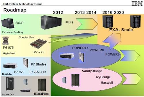
IBM Power roadmap, 2011 through 2020
The next Power roadmap below doesn't really tell you much new except that IBM is internally calling the Power Gen2 processors that were announced last October Power7': Power Seven Prime. Never saw a prime symbol before added to a chip, but why not? IBM was adamant about not calling it Power7+, even though some of its own executives did so.
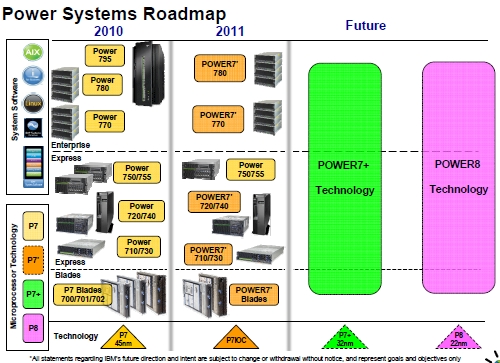
IBM's Power7 and Power 8 roadmap, circa October 2011
Here's another new one that I stumbled across that I think you will enjoy:
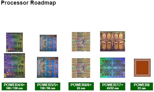
IBM Power server chips over time
This one shows the die shots of all the Power processors in the family - and to my amazement, also includes the Power7+ chip that has not been announced yet. A few things are immediately obvious from this chart. First, the Power4+, Power5+, and Power6+ chips were essentially unchanged compared to their Power4, Power5, and Power6 predecessors. And the Power6+ chips were a big disappointment since IBM missed the 45 nanometer shrink it had been expecting to add features to the chip and boost clock speeds. As you know, IBM didn't even call the Power6+ chips by the right name because it was trying to not talk about whatever issues the company was having with the 45 nanometer shrink.
Let's zoom in on those Power7 and Power7+ chips in that chart.
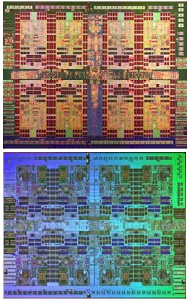
Power7+ gets topsies, Power7 get bottomsies
That's the Power7 on the bottom in its 45 nanometer process and the Power7+ on top in its 32 nanometer process. I flipped the orientation of the Power7 chip horizontally so the parts would map correctly. (You can see the original image of the Power7 chip I published back in February 2010 here, and you can see this is the same image as in this Power chip roadmap chart.)
Power7+ is a very different processor, not just a shrink, and that is probably why it is coming about six months later to market than IBM planned. (Power7 was due in May 2010 but was pulled ahead to February of that year because of Intel's "Westmere" Xeon 5600 launch.)
You can see that the Power7+ design wraps each core in L3 cache memory. Every nook and cranny of the chip is packed with L3. It looks like the L3 cache and chip core interconnect at the center horizontally in the chip is essentially the same. The local SMP links for the cores on the chips, which run along the top of the chip and halfway down the center middle and the right edge of the chip look largely unchanged, as do the remote SMP links and I/O links along the bottom edge and reaching up to the center middle. The two DDR3 memory controllers are on the outside edges, nestled between the SMP and I/O circuits.
For fun, I took an image of the Power7 core with its various elements and put it next to a zoom in on the rather low-resolution Power7+ chip image, and here's what it looks like when I tried to map out the chip elements to the Power7+ chip:
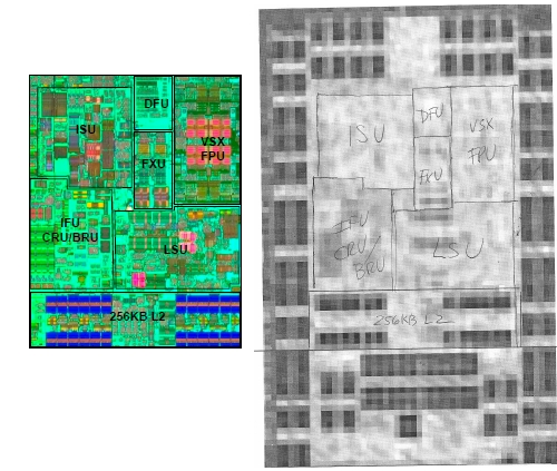
IBM Power7 and Power7+ cores
At the bottom of the chip is the 256 KB of L2 cache memory. Above that on the right are two load store units (LSU) and a condition register unit (CRU), a branch register unit (BRU), and instruction fetch unit (IFU). Each Power7 core has 32 KB of L1 instruction cache and 32 KB of L1 data cache. The instruction scheduling unit, which is where the out-of-order execution in the chip gets handled is on the top right. On the top right are four double-precision vector math units, and in the top middle are the two fixed point units (FXU) and above that is the decimal fixed unit (DFU) that does two-digit money math. I took a stab at carving up the Power7+ core, and you can see, there is not that much different.
But, if you look carefully and take out the extra L3 cache memory wrapped around each core, you can see there is indeed some room at the top and the bottom of the chip for extra goodies. These must be the accelerators that IBM is talking about in the roadmap.
Some intrepid readers who keep track of the updates to the Linux kernel gave me a bit of help on what these might be. In this post at the Linux kernel drive database, we see that the Power7+ will have an n-nest cryptographic accelerator that supports the Advanced Encryption Standard (AES) encryption algorithm as well as the Secure Hash Algorithm-2 (SHA-2) functions developed by the National Security Agency in the United States. (Hash functions are used all over the place in code and microcode alike.) Here's another link at the Linux-Crypto site that talks about driver support for an on-chip AES accelerator. Intel's Xeon 5600, E5, and E7 processors support AES encryption and decryption, and Oracle's Sparc T4, announced last fall, supports both AES encryption and SHA-1 and SHA-2 hashing functions, among a slew of other encryption and hashing.
And here is yet another link that suggests there will be a random number generator etched onto the Power7+ processor. RNGs are also an important part of many applications, particularly in any kind of simulation that depends on, er, randomness, such as those in financial services or physics.
Undoubtedly more mysteries will be revealed about the Power7+ chip at the Hot Chips 24 conference by IBM. I am looking forward to it. ®