Original URL: https://www.theregister.com/2012/06/07/review_amd_and_nvidia_extreme_gpus/
AMD and Nvidia extreme GPUs workout
Visual feast
Posted in Personal Tech, 7th June 2012 06:00 GMT
Extreme PC Week

At the very extreme end of desktop graphics are the dual GPU, frame crunching, power hungry monsters that you won’t give you much change from a grand. The extreme offerings can be a little difficult to find too, as most card vendors only produce a limited range. Instead, they prefer to concentrate on the next rung on the ladder down, the high-end cards, before turning to the real bread and butter part of the market; the entry-level cards.
Yet the extreme end of innovation is the ground where the two giants of the dedicated graphics architecture design, AMD and Nvidia, slug it out. In the most recent bout of high-end graphics technology launches, AMD turned up with its Southern Islands architecture in December 2011 and Nvidia was nowhere to be seen. In fact it was only in March 2012 that Nvidia could respond to AMD’s baiting with cards built around the new Kepler architecture, that we'll come to shortly.
AMD Southern Islands
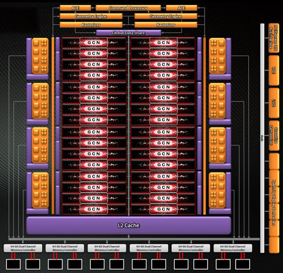
AMD’s Southern Islands architecture takes care of all its 7000 series cards and is the first to implement the company’s Graphics Core Next (GCN) technology. The single GPU flagship of the range uses the Tahiti core better known to you and me under its marketing moniker of the Radeon HD 7970.

AMD Radeon HD 7970 Tahiti block diagram
Built on a 28nm process, the world’s first GPU to do so, it has no less than 4.3 billion transistors squeezed on a die that is some 365mm². Now 4.3 billon transistors sounds OK if you say it quickly enough but let’s try to put this into some kind of perspective. Take Intel’s current top of the range Ivy Bridge processor, the Core i7-3770K, has just 1.4 billion on a 160mm² die. Yup, this AMD chip is a monster. It also lays claim to another couple of firsts: the first graphics core to support DirectX 11.1 and the first to support PCI-E 3.0.
Clock speeds for the HD 7970 are 925MHz for the core with 2048 Stream Processors running at the same rate. The huge 3GB of GDDR5 memory runs at 1,375MHz or an effective memory speed of 5.5GHz. The graphics RAM utilises a 384-bit memory bus, giving the HD 7970 something in the region of 264GB/sec of bandwidth.
AMD’s multi-monitor technology gets a boost in the Tahiti core – Eyefinity Version 2.0 supports monitors of different sizes and resolutions, allowing custom resolutions to be created too.
Nvidia Kepler
Kepler’s predecessor was codenamed Fermi and it’s an understatement to say that it had a difficult birth. Still, all credit to Nvidia though, it stuck with Fermi and turned out some very good graphics cards with later incarnations of the architecture. A feat that a great number of people thought impossible having played around with the first examples of it. Not wishing to make the same mistake twice, the Nvidia took its time to unleash Kepler. Time, that was presumably well spent keeping an eye on what AMD was doing with its 7000 series.
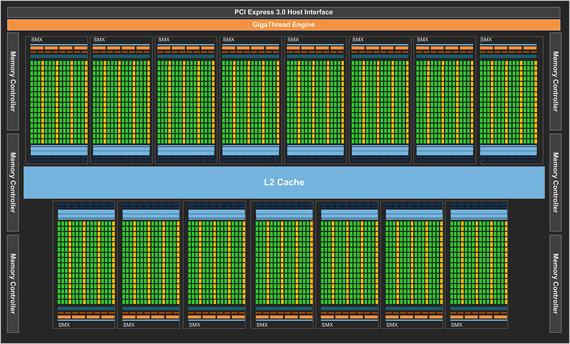
Like AMD’s Southern Island’s architecture, Kepler is built using a 28nm process but is a much smaller chip at just 295mm², but then it does have a lower transistor count at 3.5 billion.
Furthermore, it’s not strictly a totally new architecture either, but more of a Fermi die shrink, tidy up and update. The upshot is its leaner, meaner and more power efficient processor. The first example of the new architecture to see daylight carries the codename GK104 but is better known as the GeForce GTX 680.
The GTX 680 has 1536 CUDA cores which is a staggering three times as many as the previous generation’s GTX 580. This massive rise is due to the fact that Nvidia has junked the shader clock and chosen to increase the number of CUDA cores to achieve the same effect.
Albeit minus the shader clock, Nividia has added a Boost Clock, so although the base clock speed is 1006MHz, the boost speed – turbo, if you like – is 1058MHz. The 2GB of GDDR5 memory is clocked at 6.008GHz and runs through a 256-bit bus giving a maximum memory bandwidth of 192.4GB/sec. So technically, that’s the how the land lies between these two gods of graphics, but back in the real world, how do these architectures fare in products you can actually buy?
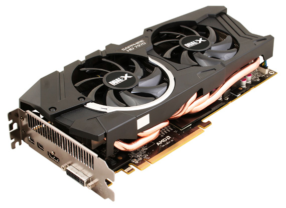
Sapphire Radeon HD 7970 Dual-X
As one of AMD’s biggest partners, Sapphire have a number of HD 7970 boards in its catalogue. One of the latest is the HD 7970 Dual-X which for around £380 comes factory overclocked and dumps the reference AMD design cooler for a neat dual fan cooling solution. Two 90mm fans sit on top of a large heatsink which takes the heat away from the core via five copper heat pipes.

Sapphire Radeon HD 7970 Dual-X
There’s a tiny two way switch on the on the top of the PCB which controls the boards two BIOSes. Yep the card comes with two BIOS’s, the first one, the standard setting if you like pushes the cards clock speeds up to 950MHz for the core and 1,475 (5.7GHz).
Push the switch to the second BIOS and things get very interesting, the speeds get even higher; 1GHz for the core and 1,450 (5.8GHz) effective for the memory, but on this setting there is the opportunity to raise the cores voltage enabling the clock settings to be pushed even further. Thankfully this mode also allows the fan speed to be increased which should help keep the card cool and stable while being overclocked.
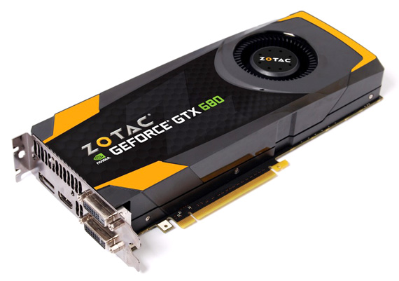
Zotac GeForce GTX 680
Zotac offers a number of variations on the GTX 680 but the basic version is the vanilla box one. Namely, for around £440 you get something that is totally as per Nvidia’s reference design, including clock speeds. The only noticeable differences are the Zotac labels and colour flashed on the cooler.

Zotac GeForce GTX 680
Until the GTX 680 emerged, AMD’s Radeon HD 7970 had its moment in the sun as the fastest single core graphics card available and as such the company had the high-end market pretty much to itself. Yet the arrival of Nvidia's GTX 680 has seriously rained on AMD's parade, taking back the title for the fastest single core card and stirring up the market at the same time.
Verdict
The game is not lost though, as it all depends on the side you take. The AMD's tech in the Sapphire delivers flexibility and value for those who want to experiment with overclocking, thanks to its very effective cooling. Alternatively, for fiddle-free performance, the Zotac Nvidia option looks appealing. That said, Zotac's GXT 680 Amp! Edition offers versatility for extreme tweaks, but you'll need to tweak your budget too. ®
Benchmark Tests
3DMark 11

1080p Extreme Preset: overall score
Longer bars are better
DirectX 11 gaming – DiRT3

1080p 4xFSAA Ultra settings: average frame rate
Longer bars are better
DirectX 11 gaming – Aliens v Predators

1080p average frame rate
Longer bars are better
