Original URL: https://www.theregister.com/2012/05/08/wtf_is_intel_ivy_bridge_architecture/
WTF is... Intel's Ivy Bridge
Inside Core i's third generation
Posted in Personal Tech, 8th May 2012 06:02 GMT
Feature

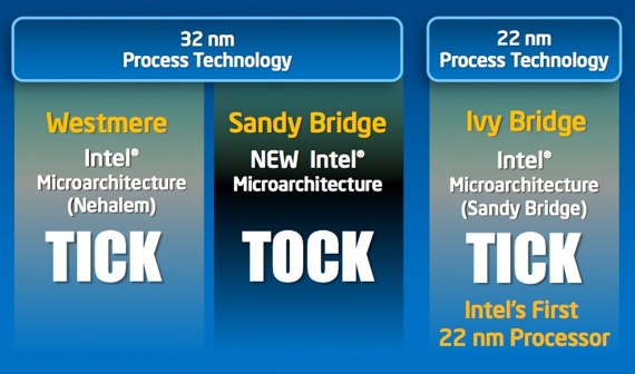
Intel’s latest processor architecture, codenamed Ivy Bridge, is its previous one, Sandy Bridge, shrunk. Sandy Bridge chips, marketed as second-generation Core i CPUs, were produced using a 32nm process. Ivy Bridge is 22nm
Actually, there's a little bit more to it than that.
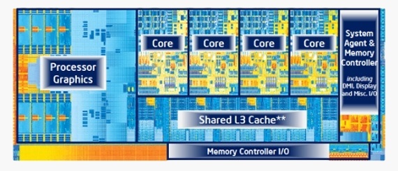
The Ivy Bridge die layout is indeed much the same as Sandy Bridge's. There are four 64-bit x86 processor cores, a memory controller and a graphics processor all integrated onto the same silicon die. Each CPU core has 64KB of Level 1 (L1) cache and 256KB of second level cache (L2) and all four cores and the graphics core share 8MB of L3 cache, called Smart Cache by Intel.
The die shrink from 32nm to 22nm allows Intel to pack in more transistors into an even smaller space. The Sandy Bridge 3.5GHz Core i7-2700K has 1.16 billion transistors on a 216mm² die. The Ivy Bridge equivalent, the i7-3770K, measures just 160mm² and contains 1.4 billion transistors - 21 per cent more.
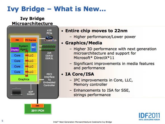
What's new, according to Intel...
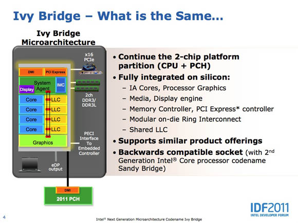
...and what is shares with Sandy Bridge
At the heart of the new fabrication process is the Intel’s Tri-Gate transistor technology, which the chip giant is calling the world’s first '3D' transistor. Traditionally, the transistors in a processor or any other silicon chip are to all intents and purposes flat, so they're considered to be 2D even though they're not literally so. The new Tri-Gate transistors have a fin that stands vertically up off the silicon substrate, hence the 3D tag.
This design helps with the real enemy of die shrinkage: electron leakage. A transistor is a switch, the on and off state determined by whether the "gate" allows current to flow from "source" to "drain".
As transistors get smaller - that 32nm and 22nm numbers the production process is named after record the size of the transistor - electrons can more easily pass through the device, even if it's turned off, thanks to the quirky properties of electrons and Quantum Mechanics.
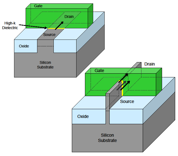
The traditional transistor design (left) and Intel's Tri-Gate structure (right). Wrapping the gate around the 'fin' channel cuts leakage
The new Tri-Gate design essentially increases the gate's surface area, making it much better at controlling electron flow - it can turn the current on and off more quickly than the traditional design can - and at reducing electron leakage.
And it allows more transistors to be added to a smaller space, which will be very useful for manufacturing even smaller dies in the future.
Graphics
Smaller transistors require less switching power, reduced further by the Tri-Gate design, which manifests itself as a lower power consumption. Using the Core i7-2700K as an example again, its TDP (Thermal Design Power) is 95W, which the i7-3770K, at the same clock frequency, knocks down to 77W.
While lowering the power consumption for the desktop chip is good, it’s really going to make a real difference in mobile, battery powered platforms.
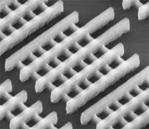
Shreddies style chips: Intel's 22nm transistors
The most significant change within Ivy Bridge's architecture is its integrated graphics processor (IGP). Probably the most important upgrade: the IGP now supports DirectX 11. Yes, it’s been a long time coming, but it’s here at last, allowing Intel's graphics to deliver the features defined by the latest incarnation of Microsoft's Windows gaming sub-system.
There are two versions of the IGP. First, there's the HD 4000, which will feature in the high-end Ivy Bridge chips. It has 16 shader units and a core speed of up to 1.15GHz. Although the core is capable of running at 1.35GHz, this higher speed will only be available to mobile CPUs.
The second Ivy Bridge IGP is the HD 2500, aimed at the mainstream market. It has a core speed of 1.15GHz too, but with just six shader units.
Both IGPs are set to run at 650MHz, but can reach the higher speeds if the need arises. Again, this is all in the name of energy preservation.
Intel has also added is hardware tessellation to the IGP, which speeds the process of breaking large areas of an image into small ones which can be textured, lit and, where possible, duplicated. It all helps the IGPs push out more pixels per second.
Intel's Wireless Display technology - think using Wi-Fi in place of an HDMI cable - is now at version 3.0, which has lower latency than before and supports two screens, thanks to the IGP's pixel-processing capabilities. The new IGP also is able to support three displays instead of two through wired links.
Intel has taken the opportunity to enhance its processors' security adding a Digital Random Number Generator (DRNG), a high speed number generator to churn out cryptographic keys quickly and less predictably than basic, pseudo-random number generators in software.
Chips and chipsets
There's also Supervisory Mode Execute Protection (SMEP) which helps to prevent Escalation of Privilege (EoP) attacks in both 32- and 64-bit operating modes.
Intel have also upgraded the cores instruction set with a couple of new conversion instructions between 16-bit floating point and 32-bit single-precision floating point numbers, which helps save memory by allowing coders to send off a few instructions to perform these commonplace calculations rather than doing it in their own code.
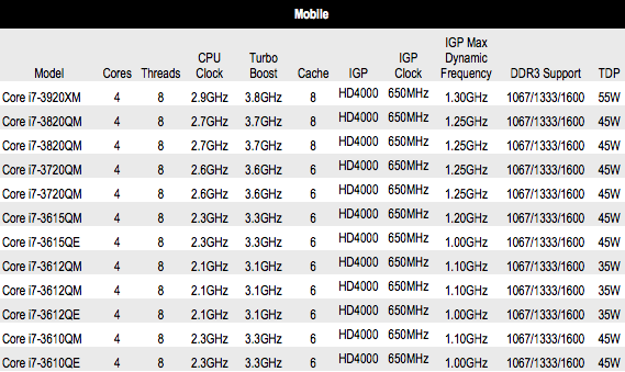
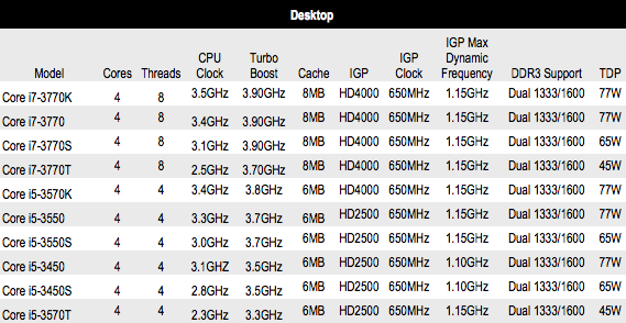
Intel’s initial Ivy Bridge line-up comprises 20 of the third-generation processors split ten each between the desktop and mobile segments.
In general, if a processor is suffixed with a K, it's unlocked for overclocking. S-class processors have a lower CPU clock and a reduced TDP, while T-branded ones have even lower core clocks, lower Turbo Boost peak speeds, and a much reduced TDP. If a core has no suffix then is a straightforward CPU aimed towards the mainstream market sector.
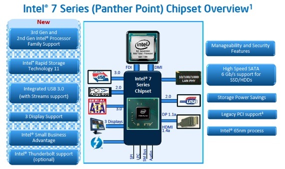
Accompanying the Ivy Bridge CPUs is a new range of chipsets, all of which were codenamed 'Panther Point' but will be marketed as the 7 series. All of them support both Ivy Bridge and Sandy Bridge CPUs. Like Sandy Bridge, Ivy Bridge chips use the LGA1155 socket, so should work in a Sandy Bridge-oriented motherboard, though you may need to update the board's Bios and even then there’s no guarantee you’ll get all the Ivy Bridge functionality.
At the time of writing, there are six new 7-series chipsets, three for the consumer market - Z77, Z75 and H77 - and three for the business sector: B75, Q75 and Q77.
All this technology is great, and it's nice to have kit that delivers more performance yet consumes less power than before. But what is the Ivy Bridge user experience really likely to be?
Well, if you already have a second-generation based system, then there’s no real point in upgrading. The new chipsets have native USB 3.0 support and PCI Express 3.0, the lanes for which come directly from the Ivy Bridge CPU, but the jury is still out on whether the jump from PCIe 2.0 to 3.0 makes any real difference, particularly when it comes to gaming.
And most existing Sandy Bridge-oriented boards have USB 3.0.
But if you're thinking about moving from an older platform then Ivy Bridge is clearly the way to go. And that's going to be even more the case when Intel rolls out mobile Ivy Bridge chips. Better graphics will reduce the need for a separate GPU, so lesser laptops will be cheaper. And the better power preservation should mean Ivy Bridge laptop users enjoy longer battery life. ®
