Original URL: https://www.theregister.com/2011/03/03/intel_poulson_itanium_isscc_followup/
Intel outs 'Poulson' speeds and feeds
Yes, more chip porn!
Posted in Channel, 3rd March 2011 04:00 GMT
ISSCC Intel has released some additional about its future eight-core "Poulson" Itanium processors.
The Poulson chips are the first Itaniums to have a new microarchitecture and core redesign since the "McKinley" cores a decade ago. As previously reported, the processor has a total of 3.1 billion transistors and is implemented in Intel's current 32 nanometer wafer baking technologies, which includes strained silicon.
The Poulson chip is 18.2 by 29.9 millimeters (544 square millimeters) and has about 20 per cent less die area than the quad-core "Tukwila" Itanium 9300 chip it will eventually replace in the lineup probably in early 2012 if Intel can stick to the two-year cadence is it trying to set for the Itaniums so Hewlett-Packard, the last big user of the Itanium chips, can keep pace with Power and Sparc upgrades.
El Reg was missing a whole bunch of information about the Poulson chip when Intel gave prebriefings ahead of the ISSCC event, but Reid Riedlinger, the chief chip engineer for the processor, filled in some gaps in his presentation at ISCCC. For one thing, Riedlinger's presentation had die shots that showed a lot of the salient features of the processor, which Intel did not provide in its briefings to the press.
So, here is what the Poulson chip looks like:
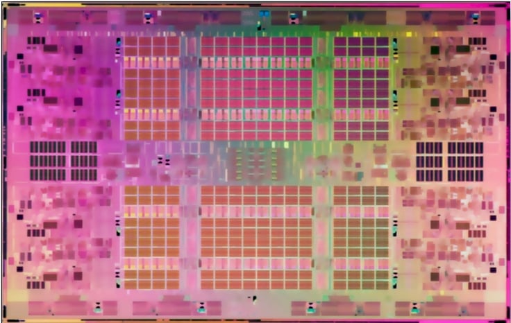
Intel's future "Poulson" Itanium processor (click to enlarge)
Like the future "Sandy Bridge-EP" and "Westmere-EX" Xeon processors from Intel, which El Reg told you all about here from ISSCC, the Poulson Itanium chip is a "cores-out" design, which means that the cores are on the outside of the chip with the shared L3 caches occupying the center of the chip.
The QuickPath Interconnect (QPI), which allows point-to-point communication between processors in adjacent sockets in a system board and across multiple systems boards in an SMP server, run along the top, and the Scalable Memory Interconnect (SMI) DDR3 memory controllers and buses run along the bottom. Here's a slightly better Poulson chip schematic than Intel was handing out in its prebriefs:
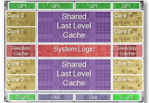
Riedlinger gave out the transistor budget for the Poulson chip, which was interesting. About 712 million of those transistors are for the cores themselves, with the remaining 2.44 billion going for the uncore portions. Most of that is, as you can see from the chip shot, used up in the shared L3 cache, which is segmented in 4 MB blocks (one per core) and linked together by a high-speed, bi-directional ring interconnect.
Riedlinger said that the core logic's 712 million transitors took up about 158 square millimeters of area, ran at between 0.85 and 1.2 volts, and burns about 95 watts. The L3 caches had 2.17 billion transistors, ran at between 0.9 and 1`.1 volts, but only burned 5 watts; the L3 caches occupied 163 square millimeters of chip real estate. The system interconnect circuits linking the cores to the L3 caches on the chip were fashioned from 22 million transistors, ate up 137 square millimeters of space, ran at the same 0.9 to 1.1 volts, but burned 50 watts. The I/O logic (QPI, memory controllers, and SMI buses) were etched with the final 44 million transistors, ate 68 square millimeters of chip area, ran at 1.05 to 1.1 voltage, and slurped 20 watts under load.
The Poulson chip has a total of 54 MB of SRAM memory on it. This includes 32 MB of L3 cache, 2 MB of total L2 data cache, 4 MB of total L2 instruction cache, 2.2 MB of director cache, 3.6 MB of last level tags, and a tiny slice (169 KB) of L2 instruction tags. Don't forget the L1 data and instruction caches on each core.
The funny bit
The one funny bit in the Poulson design are the two half-QPI links at the bottom of the chip. These were added, accoording to Riedlinger, to provide glueless interconnections for eight-socket machines. Iit would not be surprising to see them used as interconnects for linking even larger systems into a single SMP image with a modified "Boxboro" chipset from Intel or a tweaked sx3000 chipset from HP, which is used in its Integrity Superdome 2 servers.
The main thing to remember about both the QPI and SMI links is that the run at 6.4 GT/sec, which is the full speed supported by the current Boxboro chipset from Intel and that is 50 per cent more bandwidth than the Tukwilas, with their 4.8 GT/sec speed, had. The Poulson processors are socket compatible with the Tukwilas, so they can plug into existing systems, which already had that faster transfer rate baked in last year. They also run at 170 watts under normal loads, compared to 185 watts for the Tukwilas.
Here is a slightly better schematic of the Poulson cores themselves:
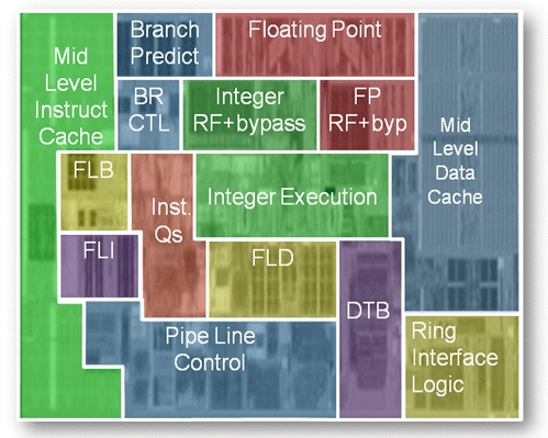
You can see all of the components clearly in this one. The Tukwila Itaniums had an eleven stage pipeline, but the Poluson cores have shrunk that down to nine stages The pipeline does instructions in order (remember, the EPIC architecture has compilers do the parallelization work so the hardware doesn't have to do out-of-order execution.) The front-ends and back-ends of this Poulson pipeline are decoupled, with the front-end able to fetch six instructions per clock and the back-end able to retire a dozen instructions per clock. The prior Itaniums could only issue six instructions per cycle. Each core has HyperThreading, but Intel has not said how many virtual threads will be on each core. (There's some chatter that Intel will jump up from two to four threads per core.)
The Poulson core has six arithmetic logic units, two integer units, two floating point units, two memory units, and three branch units that are distributed across twelve ports. Each core has 16 KB of L1 instruction and 16 KB of L1 data cache, with 512 KB of L2 instruction cache and 256 KB of L2 data cache. Then there is 4 MB of L3 cache per core, but these L3 caches are shared across the cores, unlike the L1 and L2 caches. Those caches all have ECC error correction.
Here's how the caches lay out on the Poulson chip:
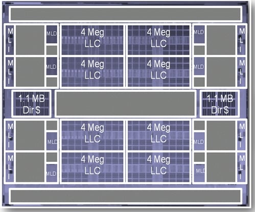
If you play a lot of Tetris, you can see that there are actually two Poulson core types, with one being a vertical mirror image of the other. There is also a horizontal reflection core (so I guess that makes four in total). This is so Intel can get the ring connect electronics and L2 data caches to line up along the inside of the chip, near the L3 caches and ring interconnect. The L2 instruction caches can be on the outside of the cores, and far away from the the L2 data and L3 caches, because the Poulson core is optimized for single-cycle integer execution against the L1 data cache. This is the kind of work that big database and ERP systems do.
Each memory controller on the Poulson chip supports two SMI ports operating in lockstep at the 6.4 GT/sec speed, and they provide a maximum of 512 GB of memory per socket. So a glueless eight-socket box will be able to support up to 8 TB of main memory, which is a hell of a lot of DDR3 DRAM. (I was going to say I was glad that I didn't have to pay for it, but we all do pay for it, one way or another, when a corporation or government buys a server, don't we?) Those memory controllers have double device data correction scrubbing.
Riedlinger said that there was an aggregate of 45 GB/sec of bandwidth from those SMI ports to memory cards in the system and 128 GB/sec of bandwidth out of those four and two halves of QPI ports. The L3 cache ring interconnect has a whopping 700 GB/sec of bandwidth.
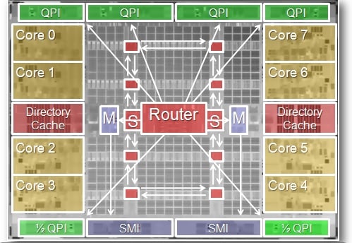
The Poulson also has a ten-port crossbar router for managing I/O and memory traffic across the chip. Here's what that looks like:
The Poulson chip has seven different power planes. Four for each pair of cores, one each for the systen I/O at the top and bottom of the chip, and one for the L3 cache and ring interconnect. By having these separate power domains, Riedlinger said that Intel could ratchet up and down the speed of core pairs without impacting the overall thermals of the chip, providing about 5 percent extra performance on the workloads it tested without impacting electricity consumption or heat dissipation. This is about as close a thing to a free lunch as you can get in the chip racket. ®