Original URL: https://www.theregister.com/2011/02/24/amd_bulldozer_core_isscc/
AMD's Bulldozer cores to push to 3.5 GHz and beyond
Big bump in oomph per socket
Posted in Channel, 24th February 2011 17:28 GMT
ISSCC Chip maker Advanced Micro Devices lifted the veil a bit on the "Bulldozer" core module at the IEEE's International Solid-State Circuits Conference in San Francisco, showing off the power savings and faster clock speeds that the new design will allow for its workstation and server processors.
As is the case with most of the enterprise processor presentations at ISSCC, the ones done by chip engineers Hugh McIntyre – who talked about the Bulldozer core module – and Michael Golden – who talked about the out-of-order scheduler and integer unit used in the chips – are full of electrical engineering goodness, a very large portion of which goes right over El Reg's head. But there are a few things that mere journos can understand, and some pretty pictures to go along with them.
First and foremost, here is the first sighting of the actual Bulldozer core module, which McIntyre showed off:
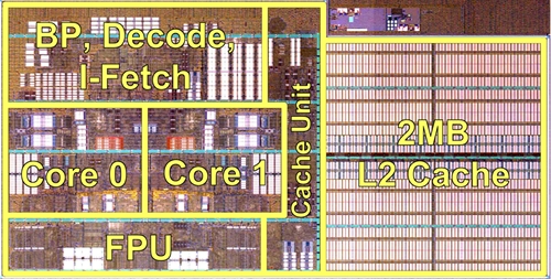
Up until this time, AMD has only been showing an abstracted block diagram of the Bulldozer module. As El Reg has previously reported, the Bulldozer core is implemented in GlobalFoundries' 32nm, 11-metal layer, high-k metal gate, silicon-on-insulator wafer-baking processes. The idea behind the core module is to have some components shared across two cores, but to give each core its own thread (with no simultaneous multithreading) to have two strong cores. Each core – which means an integer unit and a floating point unit – in the Bulldozer module has its own integer unit scheduler and L1 data caches, but the cores share fetch and decode units as well as a floating point scheduler and L2 cache memory.
The Bulldozer modules are cookie-cuttered in two-core units, and the future "Valencia" Opteron chip will be four of these modules with a shared memory controller, L3 cache, and northbridge spanning the four modules and eight cores. Here's what the Valencia chip, presumably to be called the Opteron 4200, looks like:
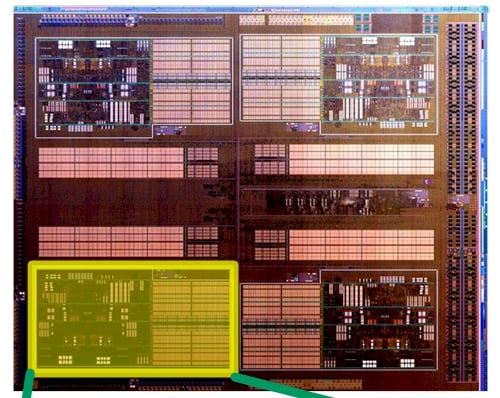
AMD has not shown an Interlagos Opteron 6200 chip, and there's a reason for that. The Interlagos chip is just two Valencias in a single package, sharing the same G34 socket.
Each integer unit in each Bulldozer core has four pipelines, capable of executing one instruction per cycle. A Bulldozer core module has two 128-bit floating point units, which can do two 64-bit double-precision operations per clock or four 32-bit single precision operations. Either core in the module can see if the other core is doing floating point math. If it is not, then one core can take all 256 bits and do four double-precision or eight single-precision ops in a single clock cycle. AMD has started calling this an AVX mode.
The Bulldozer module has 2 MB of L2 cache memory and has a total of 213 million transistors, according to McIntyre. The module has an area of 30.9 square millimeters and is designed to run at between 0.8 to 1.3 volts. Here's a zoom into the Bulldozer core module:
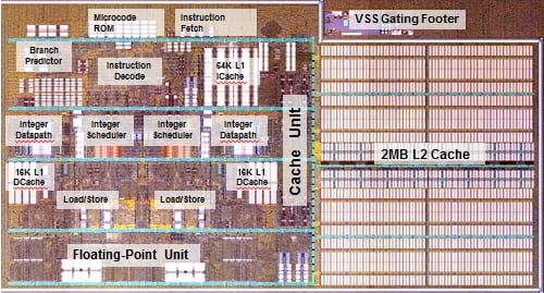
As you can see, the module has a 64 KB L1 instruction cache that is shared by both cores in the Bulldozer module, with each core having its own 16 KB L1 data cache and load/store units. The module has a shared microcode ROM, and the cores share a branch predictor, instruction fetch, and instruction decode units. The white line around the chip is a trough that allows for power to be completely shut down to each core module. So it looks like AMD will be gating power at the module, not the core level. It is not clear how this will compare to chip designs that are going to be gating at the core level.
The scheduler is capable of holding 40 entries and can issue four instructions per cycle and wake up on a single cycle. The floating point unit has new multiply-accumulate functions and supports a slew of new instructions, including SSE3, SSE4.1, and SSE4.2 SIMD extensions, on-chip AES encryption/decryption, XOP and PCLMULQDQ, which is used to perform a carry-less multiplication of two 64-bit integers.
McIntyre said that AMD was particularly proud of the power-saving features of the Bulldozer design and how it stacks up to the cores used in the current Opteron 4100/6100 processors. Here's how the chips compare:
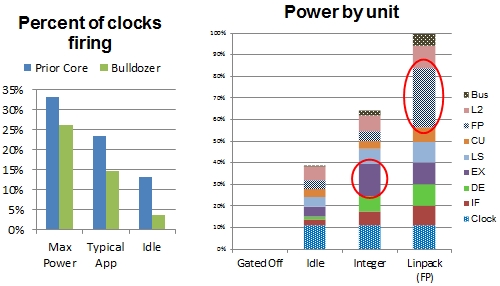
On the left, you can see how the clocks are a lot less busy, supporting the same applications with the Bulldozer design rather than with the "Lisbon" and "Magny-Cours" cores. The chart on the right shows the power budget by core component type when the Bulldozer core is gated, running idle with no work, supporting an integer workload, or running an intense floating point benchmark (in this case the Linpack Fortran test).
Here's how the power budget on the Bulldozer core module works out when it is running at 1 volt at a 100°C temperature according to AMD's initial benchmark tests:
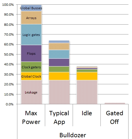
The interesting bit in this chart is that power leakage in the circuits consumes 23 per cent of the maximum power budget for the module; another 10 per cent is used for the global clocks on the module to synchronize the components. So there is not really much more AMD can do to reduce the idle power using GlobalFoundries' 32 nanometer processes. The power gating, as the chart shows, takes the core down to a fraction of the max power – you can barely see it. The other interesting piece of information is that on a typical workload, the Bulldozer module will run at about 63 per cent of maximum power.
McIntyre said that AMD was targeting clock speeds of 3.5 GHz and higher with the Bulldozer cores within the same power envelop as the current Opteron 4100 and 6100 processors. AMD just cranked the clocks on the Opteron 6100s last week, pushing up the 12-core Opteron 6180 SE to 2.5 GHz and the eight-core Opteron 6140 to 2.6 GHz using a 45-nanometer process that has run completely out of gas. The top-end Opteron 4184, which has six cores, runs at 2.8 GHz.
It would be very interesting to see AMD boost clock speeds on its 16-core "Interlagos" chips to 3.5 GHz right out of the chute late this summer while also boosting the core count by 25 per cent. With a 40 per cent boost in clock speed, that would yield an aggregate performance boost of 75 per cent per socket in the same power envelope. AMD needs that kind of leapfrog in performance and performance per watt to get the attention of server makers and their customers. I doubt very much that AMD can hit 3.5 GHz or more with the initial Interlagos Opterons, but maybe AMD can surprise the market in a good way this time around. ®