Original URL: https://www.theregister.com/2009/10/28/pcms_announcement/
Intel touts NAND-killer breakthrough
Big changes for phase changes
Posted in Channel, 28th October 2009 17:26 GMT
Intel and chip-tech house Numonyx unveiled a new technology on Wednesday that the companies claim will enable non-volatile memory to break through NAND's 20nm barrier and scale down to process sizes as tiny as 5nm - and do so cost-effectively.
What's more, the resulting stacked memory arrays could potentially usurp current DRAM and NAND-storage chores. As explained to reporters this morning by Al Fazio, Intel Fellow and director of memory technology development, this could even allow system designers to "collapse some of the DRAM and some of the storage attributes of solid state into one memory class."
In simple terms, that would allow the bringing together of DRAM and storage into one high-speed, high-bandwidth architecture. But such a leap is a long way off - products based on today's announcement won't appear for "many years," according to Fazio.
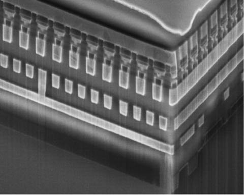
The breakthrough described by Fazio and Greg Atwood, senior technology fellow at Numonyx, is an advancement of phase-change memory (PCM) technology called PCMS (phase change memory and switch) that creates thin-film memory cells and their controlling thin-film selectors out of the same basic chalcogenide-family material and marries them together in a crosspoint architecture.

This new phase-change technology may some day blend your memory and storage into one happy family
This new thin-film selector, dubbed an Ovonic Threshold Switch (OTS), allows the stacking of multiple iterations of the memory/selector layers on a CMOS base to create high-density, high-bandwidth PCM memory.
Well, such stacking is the goal. Wednesday's announcement was of a working 64Mb, single-layer version of the new memory architecture that will make its official debut in a paper to be presented at this December's 2009 International Electron Devices Meeting in Baltimore, Maryland.
But multiple layers of the new devices are on the drawing board. As Atwood said, "The first layer is the hardest layer."
The advantages of PCM over current NAND memory are legion, according to Fazio and Atwood. For one, the electron count in a NAND cell shrinks each time the process size shinks - and it's currently down to "a handful," according to Fazio. What's more, internal voltages in a NAND cell run to over 20 volts, creating pesky interference from the resulting electric fields.
PCM, on the other hand, is read not by a charge but by the resistance of its state - either crystalline or amorphous. What's more, PCM bits are "RAM-like" in that they can be changed individually, and not merely in blocks as is required by NAND, according to Atwood.
The advantages of RAM-like capabilities are clear - at least to Fazio: "You have a memory technology that looks like memory - in other words, hardware can do a load/store because it can act on a small chunk of data with a low latency, yet it's non-volatile so that it has the non-volatile aspects of storage."
Sounds like a win-win to us - especially as Moore's Law pushes those process numbers down into the 5nm range, and the technology announced today is developed into cost-effective, high-density packages.
Fazio and Atwood have no doubt that it will. ®