This article is more than 1 year old
Much more Moore's Law: Wonder-stuff graphene transistor trickery
But this time it's a gardening job
Scientists have developed a way to “chemically grow” transistors that are only a few atoms thick in a bid to give poor old battered Moore's Law another reprieve, according to new research published in Nature Nanotechnology.
Packing more transistors on a microchip becomes increasingly difficult as shortening the distance between conductive channels increases the likelihood of current leakage.
Moore's Law, the prediction that the number of transistors can be doubled every two years, is being stretched to its limits. Intel, the world’s leading microchip manufacturer, has had to delay the release of its 10-nanometer chips as the fabrication process has proved trickier than expected.
A team of researchers led by the US Department of Energy's Lawrence Berkeley National Laboratory has attempted to solve the problem using graphene. Conductive channels were etched into a sheet of graphene on top of silica and seeds of molybdenum disulphide (MoS2) molecules were planted in the channels exposed with silica.
The molecules start to cluster around the graphene edges and fill the blank channels, creating a thin layer of MoS2 semiconductor on top of the silica.
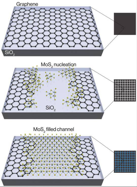
Photo credit: Nature Nanotechnology
Graphene, a material discovered in 2004, is made entirely out of carbon atoms and has very high electrical conductivity. The graphene-MoS2 edges create a transistor junction where spin current can be injected into graphene.
The two-dimensional structure stretches to a few centimetres long and a few millimetres wide. The junction measures approximately 100 nanometres across and is an overlap of single-layer MoS2 on top of graphene.
"This is a big step toward a scalable and repeatable way to build atomically thin electronics or pack more computing power in a smaller area," says Xiang Zhang, a senior scientist in Berkeley Lab's Materials Sciences Division who led the study.
Previous graphene-based transistors have been harder to fabricate. Researchers have had to manually assemble transistors, which requires precise placement and using complex fabrication techniques to create circuits.
The new technique, however, allows scientists to grow transistors on a large scale. The individual domains of MoS2 merge to create a polycrystalline single layer on top of the silica.
Zhang and his team also showed that their structure could be assembled into an inverter logic gate, which turns ones to zeros and zeros to ones in binary.
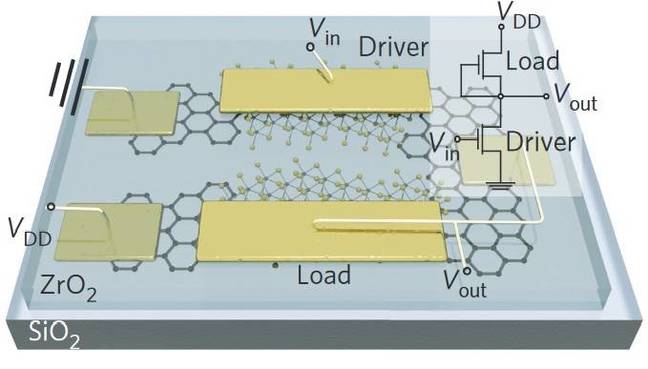
Photo credit: Nature Nanotechnology
Logic gates are key to programming computers in binary. The construction of a logic gate lays the foundation for a “chemically assembled atomic computer”, the scientists said.
“By integrating our technique with other growth systems, it's possible that future computing can be done completely with atomically thin crystals," said Mervin Zhao, a lead author and PhD student in Zhang's group at Berkeley Lab and University of California, Berkeley. ®
