This article is more than 1 year old
New research: Flash is DEAD. Yet resistance isn't futile - it's key
Electro-boffin may have SAVED the storage WORLD
Flash is at a crossroads. It cannot keep shrinking dies because, beyond a certain point, NAND cells produce too many errors, are slower to respond and have a shortened working life. Yet a University of Michigan professor's research may hold the key to the future of flash storage technology.
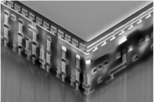
Flash foundry suppliers are working on vertical layer stacking to cram more cells at current geometries onto the same die footprint. This is exemplified by Samsung's V-NAND.
But the suppliers know that vertical layer stacking will reach its limit in turn. Once they reach that point where will they go to keep increasing density and so growing sales?
Several post-NAND technologies are in development. One uses Phase Change Memory (PCM), which features an electrical current changing the nature of a Chalcogenide substance from an amorphous state to a crystalline one and back again. Each state has a different resistance level, meaning these levels can be detected and signal binary one and zero.
Another technology is called Resistive RAM (ReRAM or RRAM) and uses the same ultimate characteristic, different resistance levels, to indicate binary values.
Such technologies promise data access speeds nearer to that of DRAM than NAND, byte instead of block addressability, and a longer working life: three much desired benefits.
Crossbar RRAM
A startup called Crossbar has demonstrated a 1MB die – although it hinted at 1 terabyte one to come - using ReRAM technology. Current NAND dies are at around the 128Gbit level so this is a huge advance. Samsung foresees a 1Tb - terabit - V-NAND die in 2017 and that's with a 96-layer die.
The die, a test die, embodies a 1TnR:1 design in which 1 Transistor driving n Resistive memory cells, more than 2,000 in the current design which, ironically, uses 3D stacking of cell layers, similar to, we understand, V-NAND's layering technology. Crossbar says this opens the road towards "commercialising terabyte scale memory arrays on a postage stamp size chip."
It claims that PCM and other RRAM suppliers' technologies suffer from a "sneak path current" phenomenon when operating in high density configurations. This hinders data access and entails using more power, Crossbar says excessively more power, than Crossbar's tech. This is based on the formation of a filament in a silicon-based switching material when a voltage is applied between top and bottom electrodes either side of the switching material.
