This article is more than 1 year old
Micron: Our stacked silicon beauty solves the DRAM problem
Logic? You want logic? It’s at the bottom
Dratted multi-core CPUs. DRAM is running into a bandwidth problem. More powerful CPUs has meant that more cores are trying to access a server’s memory and the bandwidth is running out.
One solution is to stack DRAM in layers above a logic base layer and increase access speed to the resulting hybrid memory cubes (HMC), and Micron has done just that.
Micron chose the Denver Supercomputing show to say it was developing HMC chips for petascale supercomputers. Other target applications include data packet processing, data packet buffering or storage, and processor acceleration - any app suffering memory bandwidth constraints.
At the show, Fujitsu showed a board from a prototype future supercomputer with HMC chips on it. Micron is also part of and has driven the creation of an ecosystem aimed at using HMC chips and interfacing to them.
HMC Primer
A DRAM chip combines memory and logic functions needed to access it. If you stack layers of DRAM chips atop each other then the logic circuits are duplicated. The HMC scheme is to subtract them from each chip and have a base logic layer at the bottom of the chip that provides functionality for every DRAM layer in the HMC.
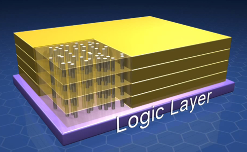
HMC schematic showing TSVs as tubes through the layers
Micron has 4- and 8-memory layer HMC initiatives. A Micron blog says: "Each memory layer has millions of memory cells in defined groups (vaults) with complex support logic (vault controller) that controls all aspects of the memory cells and provides an interface to the internal crossbar switch .... HMC has 16 vaults that operate independently of each other and are designed to sustain 10 GB/sec (80 Gb/sec) of true memory bandwidth from each vault. The logic layer also supports the external interfaces, cross-bar switch, memory schedulers, built-in self-test (BIST), sideband channels, and numerous reliability, availability, and serviceability (RAS) features."
The logic layer links or talks to each DRAM layer by using tunnels up through the structure, so-called Through-Silicon Vias (TSVs). This provides much fun for manufacturing process designers as the length of a TSV to link base and layer 3 is not that much different from one linking the base to layer 4. Controlling manufacturing precision will be vital, especially as the cost of have a defunct multi-layer die through a VIA dimension mistake will be greater than with single-layer DRAM wafers.
These TSVs have to be perfectly insulated from the DRAM layers they pass through – another tricky manufacturing skill.
A third point: where TSVs pass through a DRAM layer there can’t be memory cells. The more layers there are, the more TSVs we expect would be needed, making the chip layer designer’s life interestingly complicated.
The term “cube” is an exaggeration; think layers of thin flakes instead:
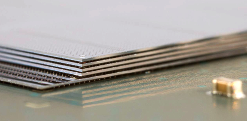
Flake city: Micron HMC chip layers
The HMC has a high-speed CPU link and the TSVs make access "massively parallel." Notes on a Micron 16-slide deck (pdf) say:
Unique DRAM within the HMC device are designed to support sixteen individual and self-supporting vaults. Each vault delivers 10 GB/sec of sustained memory bandwidth for an aggregate cube bandwidth of 160 GB/sec. Within each vault there are two banks per DRAM layer for a total of 128 banks in a 2GB device or 256 banks in a 4GB device. Impact on system performance is significant, with lower queue delays and greater availability of data responses compared to conventional memories that run banks in lock-step.
Micron says its HMC, with up to 160GB/sec, has up to 15x the bandwidth of a DDR2 module and uses up to 70 per cent less energy per bit than existing technologies. It also occupies almost 90 per cent less space than RDIMMs.
HMC ecosystem
There is an HMC consortium with eight lead developers: Altera, ARM, IBM, SK Hynix, Micron, Open-Silicon, Samsung and Xilinix. An HMC 1.0 spec has been drawn up and released, and there are more than 100 HMC adopters listed by the consortium.
The adopters can use HMC as “near memory” mounted close to the processors using it, or as “far memory” featuring scale-out HMC modules and better power-efficiency.
Micron has worked with Altera to integrate the latter’s FPGA silicon to an HMC chip and a board picture has been provided to show what’s been done:
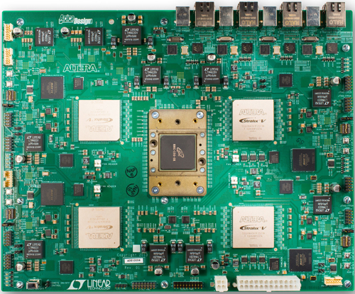
Altera board with FPGAs linked to central HMC
There’s a set of blogs on Micron’s site about HMC. Start here – it will link to the others. The Micron HMC 16-slide deck (PDF) is a good read too.
Micron is sampling its 2GB HMC chip now; a 4GB chip will sample early in 2014; and volume production of 2GB and 4GB HMC devices should occur later in 2014. ®
