This article is more than 1 year old
If tardy chip-baking fix fails, this Frenchman can help
No EUV? Carve up chips with e-beams or teach them to build themselves
SEMICON 2013 Extreme ultraviolet lithography – EUV – may be worshipped as the savior of Moore's Law by most members of the chip-baking community, but there's at least one free-thinking heretic in the semiconductor research community who refuses to be seduced into its short-wavelength, process-shrinking creed.
"I'm not working on EUV at all. Absolutely not, because I don't believe in it," said Laurent Miller, CEO of Leti, the nanotechnologies arm of the French research-and-technology organization CEA, on a panel of top researchers at the SEMICON West 2013 conference in San Francisco this week.
Miller's point of view differed radically from that of his fellow panelists. Daniel Armbrust, president and CEO of the research consortium Sematech, for example, called the oh-so-late lithographic process "essential," saying "EUV must happen."
Luc Van den hove, CEO of the Belgian nanoelectronics research center Imec joined Armbrust on the advanced lithography bandwagon. "We clearly believe that, as we all know, lithography is the enabling technology, which has been enabling scaling for many decades."
Maybe so, but current optical lithography – called 193i for its 193-nanometer wavelength and the fact that it uses a liquid immersion technique to better refract its beam – will be unable to drive down the sizes of chip features as required by Moore's Law. EUV, with its wavelength of around 13.5nm, is its long-awaited successor, but it's late – and getting later.
Heretic Miller doesn't fault his EUV-researching fellows. "These guys are doing tremendous jobs," he said. It's just that he'd prefer to take another route into the future – not only because the industry needs something to fall back on if EUV comes a cropper, but also because when EUV arrives, it ain't gonna be cheap – although, all things such as mask multiplication and defect detection considered, it's likely to be cheaper than driving 193i much further.
"And so our focus lately is more about e-beam," Miller said, referring to a chip-etching technology that doesn't used optical lithography with dozens of complex, expensive masks, but instead etches features onto silicon (and perhaps an epitaxy, a deposit of other elements) directly by the use of tightly controlled electron beams. One might even say insanely tightly controlled electron beams.
"We are committed to make an e-beam solution emerge with a reasonable throughput of typically 100 wafers per hour in the next three years," Miller promised.
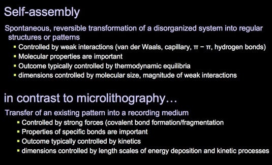
Neither is Miller putting all his chip-baking eggs in one basket. "The other thing is DSA – directed self-assembly – where we are also putting a lot of effort," he said. DSA, in a nutshell, is a way of getting existing materials to assemble themselves into patterns rather than etching those patterns into a material, as does lithography.

DSA has a pro-union mantra: 'Organize!' (source: IBM Almaden Research Center)
Miller suggests that DSA would not replace optical or even e-beam lithography, but complement them. "By mixing and combining these two approaches," he said, "we should be able in the next two or three years to start to reduce some of the wafer-processing costs."
He also takes a bit of a contrarian approach to the industry's embrace of the 3D vertical-gate transistor architecture called FinFET (Intel calls its implementation "Tri-Gate"). "We must not think of being dogmatic and say there is one single path," he said.
He's not alone on his second path, however – that path being paved with fully depleted silicon-on-insulator (FD-SOI) planar transistors. STMicroelectronics has done some great work in this area – this February, for example, they announced a 28nm FD-SOI chip humming along at 3GHz.
FD-SOI has the advantage of making life easier for chip designers, since it's simpler to transition designs intended for earlier chip-transistor architectures to FD-SOI than it is to transition them to FinFET. "Way easier," says Miller. How much further FD-SOI can be shrunk is not yet known, but he's hopeful that he and his Leti team can take this lower-cost, easier-to-use tech down to 10nm.
And being a free-thinker, he's not the kind of guy you can easily dissuade from trying. ®
