This article is more than 1 year old
IBM to double-stuff sockets with power-packed Power7+
Big boost in clock speed, smart accelerators
Giving workloads and algorithms their own special sauce
IBM's roadmaps have said that the company would use some of the Power7+ transistor budget to bolster the throughput of the chip on very precise algorithms, and Taylor showed off a bunch of them at Hot Chips.
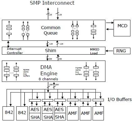
How various accelerators hook into the Power7+ chip
Each chip has three Asymmetric Math Function (AMF) accelerators, which implement math functions used in RSA and ECC cryptography. The AMF units do RSA encryption at 512, 1024, 2040, and 4096 bits, and there are ten bit levels supported for elliptic curve cryptography encryption and decryption.
Each chip also has three accelerators to handle Advanced Encryption Standard (AES) encryption with key lengths of 128, 192, and 256 bits, and to do Secure Hash Algorithm processing with SHA-1, SHA-256, SHA-512, and MD5 variants supported.
The chip also has a "true hardware entropy generator" – or random number generator – that Taylor says cannot be algorithmically reverse-engineered. This, of course, will be particularly useful for any simulation or security code that requires random numbers.
Each chip also has a special circuit, called an MCD (not sure what that's short for – Mighty Confusing Doohickey, perhaps?) that predicts if memory accesses will be on-node or off-node when they are done on a multiple socket machine.
Finally, the Power7+ chip has two special accelerators called 842 units that implement a proprietary compression algorithm that is used in the Active Memory Expansion main-memory compression that debuted with Power7 systems running AIX and that could often double the effective main memory of an AIX box.
Now that this 842 accelerator, which can do 8 bytes of compression or decompression per bus cycle, is on the iron, maybe IBM can transparently offer support for IBM i and Linux as well as AIX – Taylor told no secrets, however. The 842 refers to the 8-byte, 4-byte, and 2-byte parsings that the algorithm supports to do memory compression.
One interesting thing in the way IBM has implemented the accelerators is that the AES/SHA and AMF units are fronted by their own I/O buffers, so that if a result that comes out of an accelerator is an input for another accelerator, it can be passed over. For example, you might encrypt data and then compress it, or uncompress data and then unencrypt it – this way, you don't have to bother the CPU scheduler until the data is ready to be shipped to the core for processing. Smart.
Fight the power
With the Power7 chips running pretty hot – at least compared to x86 chips and thanks to those high clock speeds mostly – IBM has to do everything it can to save juice in its Power Systems.
With the Power7+ chips, IBM has created new power states that make it run more efficiently than its predecessors while also delivering that higher performance.
The Power7 chip had a nap mode, which allowed IBM to stop the clocks on one processor core's execution engines and leave all of the L2 and L3 cache segments associated with that core running. This nap mode was optimized so a core could be awakened quickly, with its cache states preserved and remaining coherent with the other caches in the system. This cut the core's power draw by around 10 per cent with around a 10 microsecond latency to wake it back up, according to Taylor. The Power7 chip also had a sleep mode, which cut power draw by about 35 per cent for a core module with a one millisecond wake-up time.
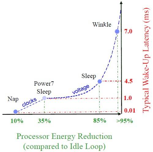
Idle states in the Power7+ processor
With Power7+ chips, IBM has a new-and-improved sleep mode and a new deep-sleep mode called "winkle" – as in Rip van Winkle, the fictional character from the Catskills region of New York where IBM is headquartered who missed the American Revolution because he slept for 20 years. Slacker.
The new sleep mode with the Power7+ chips purges the cores and their L2 caches, but leaves the shared L3 cache running in its current state. This mode cuts the power draw from the core module by 85 per cent, but takes 4.5 milliseconds to wake up. The winkle mode purges the L3 cache segment most closely associated with the chiplet, and powers off the whole core module, including core, L2 cache, and L3 cache segment. This reduces the power draw by 95 per cent, but it takes 7 milliseconds to wake the Power7+ core module back up.
Milliseconds seems like a lot of time to wake up from a low power state, so maybe the Power7+ is like the rest of us and is a little groggy after days in Hot Chips meetings.
Taylor was hassled about the long time de-winkling takes, but said this was IBM's first stab at it and that he believes the power-saving modes will be improved. ®
