This article is more than 1 year old
Graphene circuits from an inkjet printer
Magic material gets yet another surprising application
Long gone are the days when the inkjet printer was the consumable that people bought for school projects and family photographs: a group of researchers from Cambridge University has added graphene-based transistors to the list of things that you can take from the output tray.
The researchers, led by Andrea Ferrari of the university’s Department of Engineering, created an ink able to deposit graphene on a flexible silicon substrate, using this year’s favourite magic material to improve the efficiency and performance of an organic semiconductor material.
While inks able to produce printable electronics aren’t new, they produce devices that are large (and therefore slow, since if electrons have to travel a bigger distance to traverse the transistor, it takes longer, and therefore switching speed is reduced).
Moreover, in the article the group has published on Arxiv, they also note that the materials now used for printable electronics are difficult to handle. “Metal nanoparticle inks are not stable in ordinary solvents … [and] also tend to oxidize after printing”.
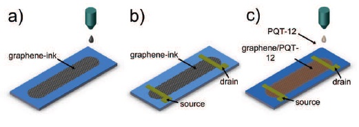
The Cambridge process deposits the graphene ink (a), then source and drain (b),
and finally the organic semiconductor (c). Source: Cambridge University.
By replacing the metal nanoparticles with graphene, the group hopes to create printable electronics on a smaller scale than is currently feasible, with fewer of these materials challenges.
The group still had to solve various challenges in handling the graphene: once microscopic flakes are chipped from a block of graphite, the resulting graphene has to be filtered to remove any particles big enough to clog the printer, and only those graphene flakes that have the right electrical properties retained; the selection of the solvent is also vital, since it needs to evaporate without leaving a perimeter residue (the “coffee ring” effect).
The solvent settled on is NMP (N-Methyl-2-pyrrolidone). In their three-step printing process, the Cambridge group first deposits the graphene onto the substrate, then adds chromium-gold source and drain pads, and finally overprints this with an organic semiconducting substance that goes by the name Poly[5,5’-bis(3-dodecyl-2- thienyl)-2,2’-bithiophene] – or PQT-12, for short.
A challenge for the future will be to come up with a cheap and efficient way to produce the graphene ink. The Cambridge lab’s three-step process: flaking the graphene into the NMP bath where it soaks for 9 hours; centrifuging the mixture for an hour to remove all flakes larger than one micron; and finally, characterizing the ink using optical absorption spectrometry, high-resolution transmission electron microscopy, electron diffraction, and Raman spectroscopy. ®
