This article is more than 1 year old
Samsung, Micron bake 3D chips for next-gen RAM
Not-particularly-cube-shaped cubes prove faster
We're hitting a memory wall, if you didn't know, and processor cores are going to be held up because DRAM can't scale up enough or ship 'em data fast enough. Samsung and Micron aim to fix that with 3D memory cubes and a consortium to define an interface spec for them.
Samsung and Micron, asserting that existing 2D DRAM architectures can't scale enough to meet the needs of higher and higher performance processors and graphics in computers and network equipment, have formed a HMC consortium (HMCC) to specify a standard cube interface. Other members are Altera, Open Silicon and Xilinx. Any adopter, OEM, enabler or integrator is free to join.
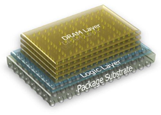
The key to this is the Hybrid Memory Cube (HMC), stacked layers of DRAM, on top of a foundation logic layer, interconnected by vertical pathways, Through Silicon Via (TSV) bonds, resulting in denser memory modules. The two reckon that a single 3D cube has 15 times the performance of a single DDR3 DRAM module, while using up to 70 per cent less energy per bit.
It's all good news here as the current sprawl of existing 2D DRAM which takes up a lot of server real estate, will be replaced by a card of cubes, meaning much more memory and using nearly 90 per cent less space than today's RDIMMs. That's what Samsung and Micron say.
Look at that another way; you could possibly get nine times more memory capacity in the same area of boards given over to thin slabs of DDR3 DRAM today.
These cubes aren't, literally, cube-shaped though, looking more like thicker slabs than current memory dies.
The consortium members expect memory cubes to be tightly coupled with CPUs, GPUs and ASICs in point-to-point configurations. It will provide tools and documentation to describe interface specifications as they develop and help their use. The spec should be delivered next year.
Will other memory suppliers join in? Elpida seems willing and, if no better ideas come along, DRAM looks set to become 3DRAM. ®
