This article is more than 1 year old
Cell phones trace family tree to rocket beams
A man, a blank pad, and some high-vacuum heat
Happy Birthday, IC "Inventing new things," says Alfred Cho, "is all about combining one technology with another to create a third."
In the mid-1960s, as a doctorate student at the University of Illinois Urbana-Champaign, Alfred Cho explored the world of surface physics. In short, he eyed the physical behaviour of materials at the intersection of two phases - a solid and liquid, say, or a solid and a vacuum.
But in the midst of this thesis, he took a job in the Space Technology Lab at TRW, the massive US defence contractor, working to build ion propulsion beams for post-Sputnik US rockets and satellites.
The two projects had nothing in common - and everything. When Cho joined Bell Labs in 1968, he somehow cross-pollinated the two, discovering a preternaturally precise method for building transistors, LEDs, and lasers. Today, molecular beam epitaxy - MBE - gives us everything from cell phone switches to the lasers driving our DVD players.
"I had my ion propulsion work - using ion beams in ultra-high vacuums to control the orbits of satellites. And I had my surface physics studies of atom arrangements on solid surfaces," Cho explains. "So I put the two together. I could grow crystals one atom layer at a time in an ultra high vacuum. I could control the thickness of devices down to atomic dimensions."
Such tight control has landed Cho in the National Inventors Hall of Fame. On Saturday night, as the integrated circuit celebrates its 50th birthday, the Hall will induct Cho alongside fourteen other IC mavens during a black-tie gala at Silicon Valley's Computer History Museum. The star-studded class of 2009 includes everyone from Intel founder Gordon Moore to George Heilmeier, the estranged father of the LCD.

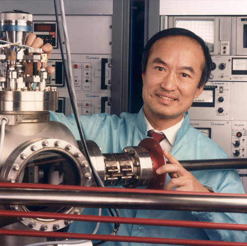
Alfred Cho: spray painting with atoms
When Cho arrived at Bell Labs in the late sixties, after completing his doctorate, he was given the sort of free rein every researcher was given. "When you came to Bell Labs, they gave you a desk and a pad of paper and a pencil and they said: 'We want you to find your own problems.'"
At the time, when building electronic devices using so-called liquid phase epitaxy, material scientists grow semiconductor crystals that were no more than 5,000 angstroms thick. But Cho's aim was to provide a far greater level of control over crystal growth - to further shrink the building blocks for the world's electronic devices. MBE was the answer.
In a high vacuum, Cho would heat up various ultra-pure semiconducting elements in so-called effusion cells, and the evaporated materials could then be applied to a substrate. With such effusion cells - akin to the thrusters at the heart of Cho's ion beam work - he would grow crystal layers no thicker than a single atom.
"Think about it as spray painting," he says. "But in this case, atoms are the paint. You're spray painting atoms onto a substrate. If you like, you can layer one kind of atom and then another - like changing colours - creating materials that don't even exist in nature."
The result is not only millions upon millions of cell phones, CD players, and DVD drives but, well, almost anything. "Now, new electronic and photonic devices are only limited by the engineer's imagination," Cho says. "If you can imagine a structure, we can make it." ®
